Epson Research and Development
Page 9
Vancouver Design Center
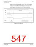
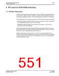
During a read cycle, OE# (output enable) is driven low. A write cycle is specified by
driving OE# high and driving the write enable signal (WE#) low. The cycle can be
lengthened by driving WAIT# low for the time needed to complete the cycle.
Figure 2-1: illustrates a typical memory access read cycle on the PC Card bus.
A[25:0]
REG#
ADDRESS VALID
CE1#
CE2#
OE#
WAIT#
D[15:0]
Hi-Z
Hi-Z
DATA VALID
Transfer Start
Transfer Complete
Figure 2-1: PC Card Read Cycle
Interfacing to the PC Card Bus
Issue Date: 01/02/06
S1D13506
X25B-G-005-03

 EPSON [ EPSON COMPANY ]