Page 18
Epson Research and Development
Vancouver Design Center
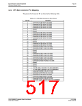
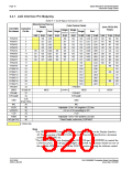
4.3.1 LCD Interface Pin Mapping
Table 4-7: LCD Signal Connector (J1)
Monochrome Passive
Panels
Color Passive Panels
Color TFT/D-TFD
Panels
Dual
S1D13506 Connector
Single Single
Pin Names
Pin No.
Single
Dual Single
Single
Format 1 Format 2
4-bit
8-bit
8-bit
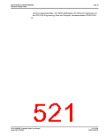
LD0
LD1
LD2
LD3
UD0
UD1
UD2
UD3
4-bit
8-bit
D0
D1
D2
D3
D4
D5
D6
D7
8-bit
D0
D1
D2
D3
D4
D5
D6
D7
16-Bit 8-bit 16-bit 9-bit 12-bit 18-bit
FPDAT0
FPDAT1
FPDAT2
FPDAT3
FPDAT4
FPDAT5
FPDAT6
FPDAT7
FPDAT8
FPDAT9
FPDAT10
FPDAT11
FPDAT12
FPDAT13
FPDAT14
FPDAT15
FPSHIFT
DRDY
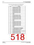
1
D0
D1
D2
D3
D4
D5
D6
D7
D0
D1
LD0
LD1
LD2
LD3
UD0
UD1
UD2
UD3
LD0
LD1
LD2
LD3
UD0
UD1
UD2
UD3
LD4
LD5
LD6
LD7
UD4
UD5
UD6
UD7
R2
R1
R0
G2
G1
G0
B2
B1
B0
R3
R2
R1
G3
G2
G1
B3
B2
B1
R0
R5
R4
R3
G5
G4
G3
B5
B4
B3
R2
R1
G2
G1
G0
B2
B1
3
5
7
D2
D3
9
D0
D1
D2
D3
D0
D1
D2
D3
D4
11
D5
13
D6
15
D7
17
D8
19
D9
21
D10
D11
D12
D13
D14
D15
23
G0
B0
25
27
29
31
33
FPSHIFT
FPSHIFT2
35 and 38
37
MOD
MOD
DRDY
FPLINE
FPSHIFT
FPFRAME
39
FPFRAME
2-26
(Even Pins)
GND
GND
N/C
N/C
VLCD
28
30
32
34
36
40
Adjustable -23 to -14V negative LCD bias
+5V or +3.3V according to JP2
+12V
LCDVCC
+12V
VDDH
NC (pin 75)2
Adjustable +24 to +40V positive LCD bias
Panel Enable, active low (LCDPWR)2
= Driven low
Note
1
For FPDATxx to LCD interface hardware connections refer to the Display Interface
AC Timing section of the S1D13506 Hardware Functional Specification, document
number X25B-A-001-xx.
The S5U13506B00C was designed using S1D13506 pin 75 (LCDPWR) to control the
LCD bias power. This design is no longer supported. Applications should use one of
the available GPIO pins to control the LCD bias power allowing for software control
2
S1D13506
X25B-G-004-06
S5U13506B00C Evaluation Board User Manual
Issue Date: 01/02/06

 EPSON [ EPSON COMPANY ]