Epson Research and Development
Page 35
Vancouver Design Center
6 Power Save Mode
The S1D13506 has been designed for very low-power applications. During normal
operation, the internal clocks are dynamically disabled when not required. The S1D13506
design also includes a Power Save Mode to further save power. When Power Save Mode is
initiated, automatic LCD power sequencing takes place to ensure the LCD bias power
supply is disabled properly. For further information on LCD power sequencing, see Section
7, “LCD Power Sequencing” on page 38.
For Power Save Mode AC Timing, see the S1D13506 Hardware Functional
Specification, document number X25B-A-001-xx.
6.1 Overview
The S1D13506 supports a software initiated Power Save Mode. Enabling/disabling Power
Save Mode is controlled using the Power Save Mode Enable bit (REG[1F0h] bit 0). The
type of DRAM refresh used during Power Save Mode can also be selected by software.
While Power Save Mode is enabled the following conditions apply.
• Display(s) are inactive.
• Registers are accessible.
• Memory is in-accessible.
• LUT is accessible.
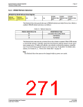
6.2 Registers
6.2.1 Enabling Power Save Mode
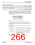
REG[1F0h] Power Save Configuration Register
Power Save
Mode Enable
n/a
n/a
n/a
Reserved
n/a
n/a
n/a
The Power Save Mode Enable bit initiates Power Save Mode when set to 1. Setting the bit
back to 0 returns the S1D13506 back to normal mode.
Programming Notes and Examples
Issue Date: 01/02/06
S1D13506
X25B-G-003-03

 EPSON [ EPSON COMPANY ]