EN29SL800
COMMAND DEFINITIONS
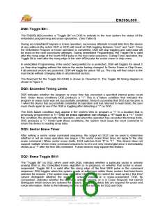
The operations of EN29SL800 are selected by one or more commands written into the command
register to perform Read/Reset Memory, Read ID, Read Sector Protection, Program, Sector Erase,
Chip Erase, Erase Suspend and Erase Resume. Commands are made up of data sequences
written at specific addresses via the command register. The sequences for the specified operation
are defined in the Command Definitions table (Table 5). Incorrect addresses, incorrect data values
or improper sequences will reset the device to Read Mode.
Table 5. EN29SL800 Command Definitions
Bus Cycles
1st
Cycle
2nd
Cycle
3rd
Cycle
4th
Cycle
5th
Cycle
6th
Cycle
Command
Sequence
Addr Data Addr Data
Addr
Data
Addr Data
Addr Data Addr Data
Read
Reset
1
1
RA
xxx
RD
F0
000
100
000
200
7F
1C
7F
1C
Word
Byte
555
2AA
555
555
Manufacturer
ID
4
AA
55
90
AAA
AAA
Device ID
Top Boot
Word
Byte
555
AAA
2AA
555
2AA
555
2AA
555
AAA
X01 22EA
X02 EA
4
4
AA
AA
55
55
90
90
Device ID
Bottom Boot
Word
Byte
555
555
X01 226B
X02 6B
(SA) XX00
AAA
AAA
Word
Byte
555
555
X02
Sector Protect
Verify
XX01
4
AA
55
90
(SA) 00
AAA
555
AAA
X04
PA
01
Word
Byte
Word
Byte
Word
Byte
555
AAA
555
AAA
555
AAA
xxx
2AA
555
2AA
555
2AA
555
555
AAA
555
AAA
555
Program
4
6
6
AA
AA
AA
55
55
55
A0
80
80
PD
555
AAA
555
2AA
555
2AA
555
555
AAA
Chip Erase
AA
AA
55
55
10
30
Sector Erase
SA
AAA
AAA
Erase Suspend
Erase Resume
1
1
B0
30
xxx
Address and Data values indicated in hex
RA = Read Address: address of the memory location to be read. This is a read cycle.
RD = Read Data: data read from location RA during Read operation. This is a read cycle.
PA = Program Address: address of the memory location to be programmed. X = Don’t-Care
PD = Program Data: data to be programmed at location PA
SA = Sector Address: address of the Sector to be erased or verified. Address bits A18-A12 uniquely select any Sector.
Reading Array Data
The device is automatically set to reading array data after power up. No commands are required to
retrieve data. The device is also ready to read array data after completing an Embedded Program
or Embedded Erase algorithm.
Following an Erase Suspend command, Erase Suspend mode is entered. The system can read
array data using the standard read timings, with the only difference in that if it reads at an address
within erase suspended sectors, the device outputs status data. After completing a programming
operation in the Erase Suspend mode, the system may once again read array data with the same
exception.
The Reset command must be issued to re-enable the device for reading array data if DQ5 goes high,
or while in the autoselect mode. See next section for details on Reset.
This Data Sheet may be revised by subsequent versions
or modifications due to changes in technical specifications.
©2004 Eon Silicon Solution, Inc., www.essi.com.tw
12
Rev. D, Issue Date: 2006/11/06

 EON [ EON SILICON SOLUTION INC. ]