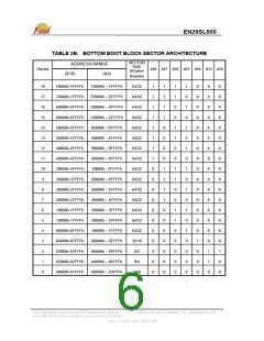
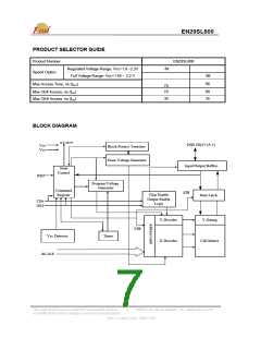
EN29SL800
To access the autoselect codes in-system; the host system can issue the autoselect command via
the command register, as shown in the Command Definitions table. This method does not require
VID. See “Command Definitions” for details on using the autoselect mode.
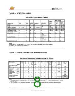
Write Mode
Write operations, including programming data and erasing sectors of memory, require the host
system to write a command or command sequence to the device. Write cycles are initiated by
placing the byte or word address on the device’s address inputs while the data to be written is input
on DQ[7:0] in Byte Mode (BYTE# = L) or on DQ[15:0] in Word Mode (BYTE# = H). The host system
must drive the CE# and WE# pins Low and the OE# pin High for a valid write operation to take place.
All addresses are latched on the falling edge of WE# and CE#, whichever happens later. All data is
latched on the rising edge of WE# or CE#, whichever happens first. The system is not required to
provide further controls or timings. The device automatically provides internally generated program /
erase pulses and verifies the programmed /erased cells’ margin. The host system can detect
completion of a program or erase operation by observing the RY/BY# pin, or by reading the DQ[7]
(Data# Polling) and DQ[6] (Toggle) status bits.
The ‘Command Definitions’ section of this document provides details on the specific device
commands implemented in the EN29SL800.
RESET#: Hardware Reset Pin
The RESET# pin provides a hardware method of resetting the device to reading array data. When
the RESET# pin is driven low for at least a period of tRP, the device immediately terminates any
operation in progress, tristates all output pins, and ignores all read/write commands for the duration
of the RESET# pulse. The device also resets the internal state machine to reading array data. The
operation that was interrupted should be reinitiated once the device is ready to accept another
command sequence, to ensure data integrity.
Current is reduced for the duration of the RESET# pulse. When RESET# is held at Vss±0.3 V, the
device draws CMOS standby current (Icc2). If RESET# is held at VIL but not within Vss±0.3 V, the
standby current will be greater.
The RESET# pin may be tied to the system reset circuitry. A system reset would thus also reset the
Flash memory, enabling the system to read the boot-up firm- ware from the Flash memory.
If RESET# is asserted during a program or erase operation, the RY/BY# pin will immediately go to a
“1” but the actual internal operations may be active until tREADY (During Embedded Algorithms: 20uS)
amount of time has passed. The system thus must wait at least tREADY amount of time after the
RESET# is asserted. If RESET# is asserted when a program or erase operation is not executing
(RY/BY# pin is "1"), the reset operation is completed within a time of tREADY (Not during Embedded
Algorithms: 500nS). The system can read data tRH after the RESET# pin returns to VIH.
Refer to the DC Characteristics tables Icc3 for RESET# parameters and to the figures at page 26 on
datasheet for the timing diagram.
Sector Protection/Unprotection
The hardware sector protection feature disables both program and erase operations in any sector.
The hardware sector unprotection feature re-enables both program and erase operations in
previously protected sectors.
There are two methods to enabling this hardware protection circuitry. The first one requires only
that the RESET# pin be at V and then standard microprocessor timings can be used to enable or
ID
disable this feature. See Flowchart 7a and 7b for the algorithm and Figure 12 for the timings.
When doing Sector Unprotect, all the other sectors should be protected first.
This Data Sheet may be revised by subsequent versions
or modifications due to changes in technical specifications.
©2004 Eon Silicon Solution, Inc., www.essi.com.tw
10
Rev. D, Issue Date: 2006/11/06

 EON [ EON SILICON SOLUTION INC. ]