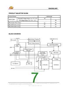
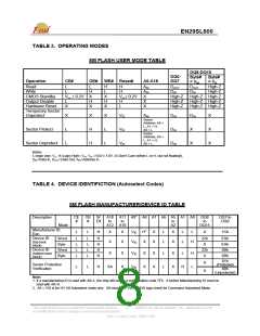
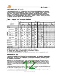
EN29SL800
The second method is meant for programming equipment. This method requires V be applied to
ID
both OE# and A9 pin and non-standard microprocessor timings are used. This method is described
in a separate document called EN29SL800 Supplement, which can be obtained by contacting a
representative of Eon Silicon Solution, Inc.
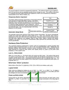
Temporary Sector Unprotect
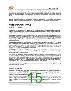
Start
This feature allows temporary unprotection of previously protected
sector groups to change data while in-system. The Sector
Unprotect mode is activated by setting the RESET# pin to VID.
During this mode, formerly protected sectors can be programmed
or erased by simply selecting the sector addresses. Once is
removed from the RESET# pin, all the previously protected sectors
are protected again. See accompanying figure and timing
diagrams for more details.
Reset#=VID (note 1)
Perform Erase or Program
Operations
Reset#=VIH
Notes:
Temporary Sector
Unprotect Completed (note 2)
1. All protected sectors unprotected.
2. Previously protected sectors protected
Automatic Sleep Mode
again.
The automatic sleep mode minimizes Flash device energy consumption. The device automatically
enables this mode when addresses remain stable for tacc + 30ns. The automatic sleep mode is
independent of the CE#, WE# and OE# control signals. Standard address access timings provide
new data when addresses are changed. While in sleep mode, output is latched and always
available to the system. Icc5 in the DC Characteristics table represents the automatic sleep mode
current specification.
Hardware Data Protection
The command sequence requirement of unlock cycles for programming or erasing provides data
protection against inadvertent writes as seen in the Command Definitions table. Additionally, the
following hardware data protection measures prevent accidental erasure or programming, which
might otherwise be caused by false system level signals during Vcc power up and power down
transitions, or from system noise.
Low VCC Write Inhibit
When Vcc is less than VLKO, the device does not accept any write cycles. This protects data during
Vcc power up and power down. The command register and all internal program/erase circuits are
disabled, and the device resets. Subsequent writes are ignored until Vcc is greater than VLKO. The
system must provide the proper signals to the control pins to prevent unintentional writes when Vcc
is greater than VLKO
.
Write Pulse “Glitch” protection
Noise pulses of less than 5 ns (typical) on OE#, CE# or WE# do not initiate a write cycle.
Logical Inhibit
Write cycles are inhibited by holding any one of OE# = VIL, CE# = VIH, or WE# = VIH. To initiate a
write cycle, CE# and WE# must be a logical zero while OE# is a logical one. If CE#, WE#, and OE#
are all logical zero (not recommended usage), it will be considered a read.
Power-up Write Inhibit
During power-up, the device automatically resets to READ mode and locks out write cycles. Even
with CE# = VIL, WE# = VIL and OE# = VIH, the device will not accept commands on the rising edge of
WE#.
This Data Sheet may be revised by subsequent versions
or modifications due to changes in technical specifications.
©2004 Eon Silicon Solution, Inc., www.essi.com.tw
11
Rev. D, Issue Date: 2006/11/06

 EON [ EON SILICON SOLUTION INC. ]