Preliminary EN29GL064
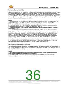
the sector. In summary, if the PPB Lock Bit is locked (set to “0”), no changes to the PPBs are allowed.
The PPB Lock Bit can only be unlocked (reset to “1”) through a hardware reset or power cycle. See also
Figure 8 for an overview of the Advanced Sector Protection feature.
Hardware Data Protection Methods
The device offers two main types of data protection at the sector level via hardware control:
•
When WP#/ACC is at VIL, the either the highest or lowest sector is locked (device specific).
There are additional methods by which intended or accidental erasure of any sectors can be prevented
via hardware means. The following subsections describes these methods:
WP#/ACC Method
The Write Protect feature provides a hardware method of protecting one outermost sector. This function
is provided by the WP#/ACC pin and overrides the previously discussed Sector Protection/Unprotection
method.
If the system asserts VIL on the WP#/ACC pin, the device disables program and erase functions in the
highest or lowest sector independently of whether the sector was protected or unprotected using the
method described in Advanced Sector Protection/Unprotection on page 26.
If the system asserts VIH on the WP#/ACC pin, the device reverts to whether the boot sectors were last
set to be protected or unprotected. That is, sector protection or unprotection for these sectors depends
on whether they were last protected or unprotected.
The WP#/ACC pin must be held stable during a command sequence execution. WP# has an internal
pull-up; when unconnected, WP# is set at VIH.
Note
If WP#/ACC is at VIL when the device is in the standby mode, the maximum input load current is
increased.
Low VCC Write Inhibit
When VCC is less than VLKO, the device does not accept any write cycles. This protects data during
VCC power-up and power-down.
The command register and all internal program/erase circuits are disabled, and the device resets to
reading array data. Subsequent writes are ignored until VCC is greater than VLKO. The system must
provide the proper signals to the control inputs to prevent unintentional writes when VCC is greater than
VLKO.
Write Pulse “Glitch Protection”
Noise pulses of less than 5 ns (typical) on OE#, CE# or WE# do not initiate a write cycle.
Power-Up Write Inhibit
If WE# = CE# = RESET# = VIL and OE# = VIH during power up, the device does not accept commands
on the rising edge of WE#. The internal state machine is automatically reset to the read mode on power-
up.
This Data Sheet may be revised by subsequent versions
or modifications due to changes in technical specifications.
©2004 Eon Silicon Solution, Inc., www.eonssi.com
38
Rev. A, Issue Date: 2009/3/20

 EON [ EON SILICON SOLUTION INC. ]