Preliminary EN29GL064
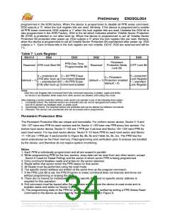
programmed in the EON factory. When the device is programmed to disable all PPB erase command,
DQ3 outputs a ‘0’, when the lock register bits are read. Similarly, if the device is programmed to enable
all PPB erase command, DQ3 outputs a ‘1’ when the lock register bits are read. Likewise the DQ4 bit is
also programmed in the EON Factory. DQ4 is the bit which indicates whether Volatile Sector Protection
Bit (DYB) is protected or not after boot-up. When the device is programmed to set all Volatile Sector
Protection Bit protected after power-up, DQ4 outputs a ‘0’ when the lock register bits are read. Similarly,
when the device is programmed to set all Volatile Sector Protection Bit unprotected after power-up, DQ4
outputs a ‘1’. Each of these bits in the lock register are non-volatile. DQ15- DQ5 are reserved and will be
1’s.
Table 7. Lock Register
DQ15-5
DQ4
DQ3
DQ2
DQ1
DQ0
Persistent
Protection Mode OTP Lock Bit
Lock Bit
PPB One Time
Programmable Bit
Reserved DYB Lock Boot Bit
Reserved
0 = protected all 0 = All PPB Erase
DYB after boot-up Command disabled
1 = unprotected all 1 = All PPB Erase
DYB after boot-up Command enabled
0 = protected
0 = Persistent
Lock Register
(default = 1)
(default = 1) Protection enabled
(default = 0)
1 = unprotect
Lock Register
Notes:
After the Lock Register Bits Command Set Entry command sequence is written, reads and writes
for Sector 0 are disabled, while reads from other sectors are allowed until exiting this mode.
After selecting a sector protection method, each sector can operate in any of the following three states:
1. Constantly locked: The selected sectors are protected and can not be reprogrammed unless PPB
lock bit is cleared via hardware reset, or power cycle.
2. Dynamically locked: The selected sectors are protected and can be altered via software commands.
3. Unlocked: The sectors are unprotected and can be erased and/or programmed.
Persistent Protection Bits
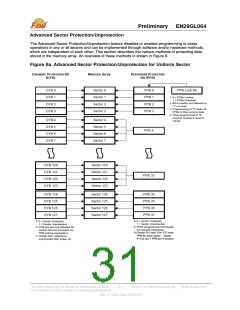
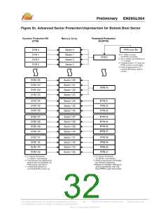
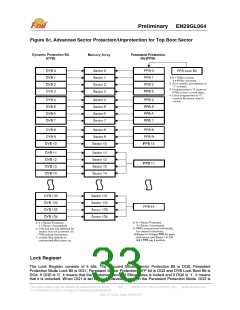
The Persistent Protection Bits are unique and nonvolatile. For uniform sector device, Sector 0~3 and
124~127 have one PPB for each sectors and for Sector 4~123 have one PPB every four sectors. For
bottom boot sector device, Sector 0~123 are 1 PPB per 4 sectors and Sector 124~134 have PPB for
each boot sector. For top boot sector device, Sector 0~10 have PPB for each boot sector and Sector
11~134 are 1 PPB per 4 sectors(refer to Figure 8a, 8b, 8c and Table 3a, 3b, 3c). The PPB has the
same endurances as the Flash memory. Preprogramming and verification prior to erasure are handled
by the device, and therefore do not require system monitoring.
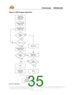
Notes
1. Each PPB is individually programmed and all are erased in parallel.
2. While programming PPB for the four sectors, array data can be read from any other sector, except
Sector 0 (used for Data# Polling) and the sector in which sector PPB is being programmed.
3. Entry command disables reads and writes for the sector selected.
4. Reads within that sector return the PPB status for that sector.
5. All Reads must be performed using the read mode.
6. The specific sector address are written at the same time as the program command.
7. If the PPB Lock Bit is set, the PPB Program or erase command does not execute and times-out
without programming or erasing the PPB.
8. There are no means for individually erasing a specific PPB and no specific sector address is
required for this operation.
9. Exit command must be issued after the execution which resets the device to read mode and re-
enables reads and writes for Sector 0.
10. The programming state of the PPB for given sectors can be verified by writing a PPB Status Read
Command to the device as described by the flow chart shown in Figure 9.
This Data Sheet may be revised by subsequent versions
or modifications due to changes in technical specifications.
©2004 Eon Silicon Solution, Inc., www.eonssi.com
34
Rev. A, Issue Date: 2009/3/20

 EON [ EON SILICON SOLUTION INC. ]