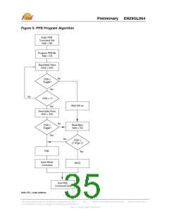
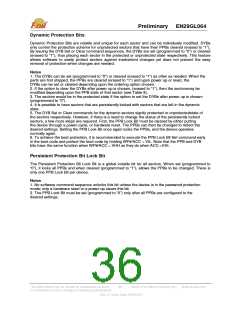
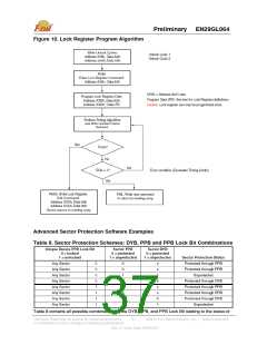
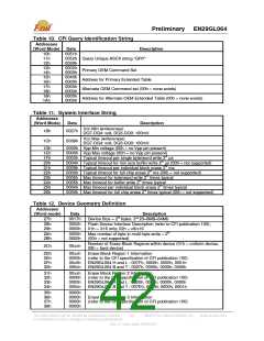
Preliminary EN29GL064
Power Conservation Modes
Standby Mode
When the system is not reading or writing to the device, it can place the device in the standby mode. In
this mode, current consumption is greatly reduced, and the outputs are placed in the high impedance
state, independent of the OE# input. The device enters the CMOS standby mode when the CE# and
RESET# inputs are both held at VCC ± 0.3 V. The device requires standard access time (tCE) for read
access, before it is ready to read data. If the device is deselected during erasure or programming, the
device draws active current until the operation is completed. ICC4 in “DC Characteristics” represents the
standby current specification
Automatic Sleep Mode
The automatic sleep mode minimizes Flash device energy consumption. The device automatically
enables this mode when addresses remain stable for tACC + 30 ns. The automatic sleep mode is
independent of the CE#, WE#, and OE# control signals. Standard address access timings provide new
data when addresses are changed. While in sleep mode, output data is latched and always available to
the system.
Hardware RESET# Input Operation
The RESET# input provides a hardware method of resetting the device to reading array data. When
RESET# is driven low for at least a period of tRP, the device immediately terminates any operation in
progress, tristates all outputs, and ignores all read/write commands for the duration of the RESET#
pulse. The device also resets the internal state machine to reading array data. The operation that was
interrupted should be reinitiated once the device is ready to accept another command sequence to
ensure data integrity.
When RESET# is held at VSS ± 0.3 V, the device draws ICC reset current (ICC5). If RESET# is held at
VIL but not within VSS ± 0.3 V, the standby current is greater.
RESET# may be tied to the system reset circuitry and thus, a system reset would also reset the Flash
memory, enabling the system to read the boot-up firmware from the Flash memory.
Output Disable (OE#)
When the OE# input is at VIH, output from the device is disabled. The outputs are placed in the high
impedance state. (With the exception of RY/BY#.)
Secured Silicon Sector Flash Memory Region
The Secured Silicon Sector provides an extra Flash memory region that enables permanent part
identification through an Electronic Serial Number (ESN). The Secured Silicon Sector is 128 words in
length and all Secured Silicon reads outside of the 128-word address range returns invalid data. The
Secured Silicon Sector Indicator Bit, DQ7, (at Autoselect address 03h) is used to indicate whether or not
the Secured Silicon Sector is locked when shipped from the factory.
Please note the following general conditions:
•
On power-up, or following a hardware reset, the device reverts to sending commands to the normal
address space.
•
•
•
Reads outside of sector SA0 return memory array data.
Sector SA0 is remapped from memory array to Secured Silicon Sector array.
Once the Secured Silicon Sector Entry Command is issued, the Secured Silicon Sector Exit
command must be issued to exit Secured Silicon Sector Mode.
The Secured Silicon Sector is not accessible when the device is executing an Embedded Program or
Embedded Erase algorithm.
•
•
The ACC function and unlock bypass modes are not available when the Secured Silicon Sector is
enabled.
This Data Sheet may be revised by subsequent versions
or modifications due to changes in technical specifications.
©2004 Eon Silicon Solution, Inc., www.eonssi.com
39
Rev. A, Issue Date: 2009/3/20

 EON [ EON SILICON SOLUTION INC. ]