Preliminary EN29GL064
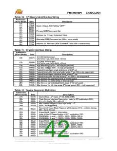
Table 10. CFI Query Identification String
Addresses
(Word Mode)
Data
Description
10h
11h
12h
13h
14h
15h
16h
17h
18h
19h
1Ah
0051h
0052h Query Unique ASCII string “QRY”
0059h
0002h
Primary OEM Command Set
0000h
0040h
Address for Primary Extended Table
0000h
0000h
Alternate OEM Command set (00h = none exists)
0000h
0000h
0000h
Address for Alternate OEM Extended Table (00h = none exists)
Table 11. System Interface String
Addresses
(Word Mode)
Data
Description
Vcc Min (write/erase)
DQ7-DQ4: volt, DQ3-DQ0: 100mV
1Bh
0027h
Vcc Max (write/erase)
DQ7-DQ4: volt, DQ3-DQ0: 100mV
1Ch
0036h
1Dh
1Eh
1Fh
20h
21h
22h
23h
24h
25h
26h
0000h Vpp Min voltage (00h = no Vpp pin present)
0000h Vpp Max voltage (00h = no Vpp pin present)
0003h Typical timeout per single byte/word write 2N µs
0004h Typical timeout for min size buffer write 2N µs (00h = not supported)
0009h Typical timeout per individual block erase 2N ms
0000h Typical timeout for full chip erase 2N ms (00h = not supported)
0005h Max timeout for byte/word write 2N times typical
0005h Max timeout for buffer write 2N times typical
0004h Max timeout per individual block erase 2N times typical
0000h Max timeout for full chip erase 2N times typical (00h = not supported)
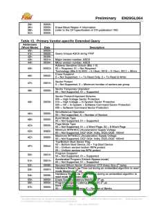
Table 12. Device Geometry Definition
Addresses
(Word mode)
Data
Description
27h
28h
29h
2Ah
2Bh
0017h
0002h
0000h
0005h
0000h
Device Size = 2N bytes. 2**23=8MB=64Mb
Flash Device Interface Description (refer to CFI publication 100);
01h = X16 only; 02h = x8/x16
Max number of byte in multi-byte write = 2N
(00h = not supported)
Number of Erase Block Regions within device (01h = uniform device,
02h = boot device)
2Ch
00xxh
2Dh
2Eh
2Fh
30h
00xxh
0000h
00x0h
000xh
Erase Block Region 1 Information
(refer to the CFI specification of CFI publication 100)
EN29GL064 H and L : 007Fh, 0000h, 0000h, 0001h
EN29GL064 B and T : 0007h, 0000h, 0020h, 0000h
31h
32h
33h
34h
00xxh
0000h
0000h
000xh
Erase Block Region 2 Information
(refer to the CFI specification of CFI publication 100)
EN29GL064 H and L : 0000h, 0000h, 0000h, 0000h
EN29GL064 B and T : 007Eh, 0000h, 0000h, 0001h
35h
36h
37h
38h
0000h
0000h
0000h
0000h
Erase Block Region 3 Information
(refer to the CFI specification of CFI publication 100)
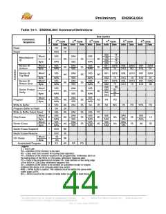
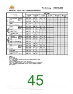
This Data Sheet may be revised by subsequent versions
or modifications due to changes in technical specifications.
©2004 Eon Silicon Solution, Inc., www.eonssi.com
42
Rev. A, Issue Date: 2009/3/20

 EON [ EON SILICON SOLUTION INC. ]