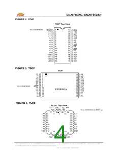
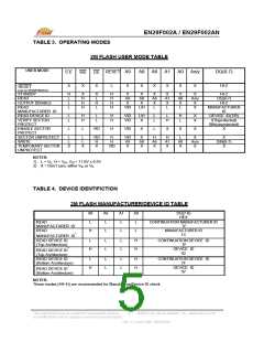
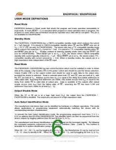
EN29F002A / EN29F002AN
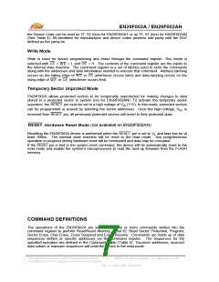
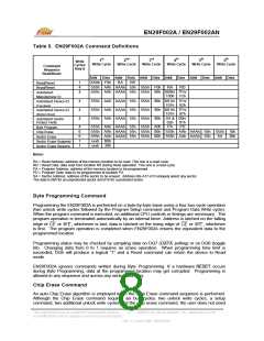
Table 5. EN29F002A Command Definitions
1st
2nd
3rd
4th
5th
6th
Write
Cycles
Req’d
Write Cycle
Write Cycle
Write Cycle
Write Cycle
Write Cycle
Write Cycle
Command
Sequence
Read/Reset
Addr Data Addr Data Addr Data Addr Data Addr Data Addr Data
XXXh F0h RA RD
555h AAh AAAh 55h 555h F0h
1
4
4
Read/Reset
Read/Reset
AutoSelect
RA
RD
555h AAh AAAh 55h 555h 90h 000h/ 7Fh/
100h 1Ch
Manufacturer ID
4
4
4
555h AAh AAAh 55h 555h 90h 001h/ 7Fh/
101h 92h
AutoSelect Device ID
(Top Boot)
555h AAh AAAh 55h 555h 90h 001h/ 7Fh/
101h 97h
AutoSelect Device ID
(Bottom Boot)
555h AAh AAAh 55h 555h 90h SA & 00h/
AutoSelect Sector
Protect Verify
02h
PA
01h
PD
4
6
6
1
1
555h AAh AAAh 55h 555h A0h
Byte Program
Chip Erase
Sector Erase
Sector Erase Suspend
Sector Erase Resume
555h AAh AAAh 55h 555h 80h 555h AAh AAAh 55h 555h 10h
555h AAh AAAh 55h 555h 80h 555h AAh AAAh 55h
SA
30h
xxxh B0h
xxxh 30h
Notes:
RA = Read Address: address of the memory location to be read. This one is a read cycle.
RD = Read Data: data read from location RA during Read operation. This one is a read cycle.
PA = Program Address: address of the memory location to be programmed
PD = Program Data: data to be programmed at location PA
SA = Sector Address: address of the sector to be erased. Address bits A17-A13 uniquely select any sector.
The data is 00h for an unprotected sector and 01h for a protected sector.
Byte Programming Command
Programming the EN29F002A is performed on a byte-by-byte basis using a four bus-cycle operation
(two unlock write cycles followed by the Program Setup command and Program Data Write cycle).
When the program command is executed, no additional CPU controls or timings are necessary. The
program operation is terminated automatically by an internal timer. Address is latched on the falling
edge of
or
, whichever is last; data is latched on the rising edge of
or
CE
, whichever
W E
CE
W E
is first. The program operation is completed when EN29F002A returns the equivalent data to the
programmed location.
Programming status may be checked by sampling data on DQ7 (
polling) or on DQ6 (toggle
DATA
bit). Changing data from 0 to 1 requires an erase operation. When programming time limit is
exceeded, DQ5 will produce a logical “1” and a Reset command can return the device to Read
mode.
EN29F002A ignores commands written during Byte Programming. If a hardware
occurs
RESET
during Byte Programming, data at the programmed location may get corrupted. Programming is
allowed in any sequence and across any sector boundary.
Chip Erase Command
An auto Chip Erase algorithm is employed when the Chip Erase command sequence is performed.
Although the Chip Erase command requires six bus cycles: two unlock write cycles, a setup
command, two additional unlock write cycles and the chip erase command, the user does not need
This Data Sheet may be revised by subsequent versions
©2003 Eon Silicon Solution, Inc., www.essi.com.tw
8
or modifications due to changes in technical specifications.
Rev. A, Issue Date: 2003/03/26

 EON [ EON SILICON SOLUTION INC. ]