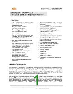
EN29F002A / EN29F002AN
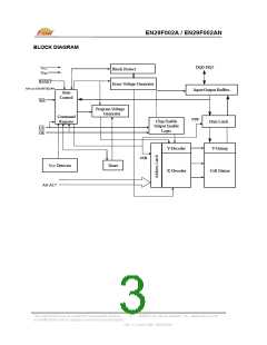
FIGURE 2. PDIP
PDIP Top View
NC on EN29F002AN
VPP
1
32
31
30
29
28
27
26
25
24
23
22
21
20
19
18
17
VCC
PGM
NC
RESET
A16
A15
A12
A7
2
WE
A17
3
4
A14
A13
A8
5
A6
A5
6
7
A9
A4
A3
8
A11
OE
9
A2
A1
10
11
12
13
14
15
16
A10
CE
A0
DQ7
DQ6
DQ5
DQ4
DQ3
DQ0
DQ1
DQ2
VSS
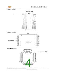
FIGURE 3. TSOP
WE
NC on EN29F002AN
RESET
EN29F002A
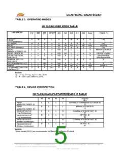
FIGURE 4. PLCC
PLCC Top View
V
A15 RESET WE
A12
A16
A17
A12 A16 VCCCC NC
A15 VPP PGM
NC on EN29F002AN at RESET pin
4
2
32
30
A7
A6
A5
A4
A3
5
6
7
8
9
29 A14
28 A13
27 A8
3
1
31
26 A9
25 A11
24 OE
23 A10
22 CE
21 DQ7
A2 10
A1 11
A0 12
DQ0 13
15
17
19
14
16
18
20
DQ2 DQ3 DQ5
DQ1 VSS DQ4 DQ6
This Data Sheet may be revised by subsequent versions
©2003 Eon Silicon Solution, Inc., www.essi.com.tw
Rev. A, Issue Date: 2003/03/26
4
or modifications due to changes in technical specifications.

 EON [ EON SILICON SOLUTION INC. ]