EN29F002A / EN29F002AN
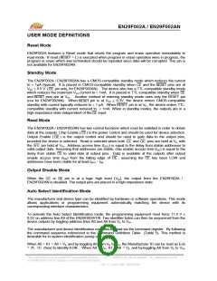
the Device Code can be read as 7F, 92 (hex) for EN29F002AT or as 7F, 97 (hex) for EN29F002AB
(See Table 4). All identifiers for manufacturer and device codes possess odd parity with the DQ7
defined as the parity bit.
Write Mode
Write is used for device programming and erase through the command register. This mode is
selected with
=
= L and
= H. The contents of the command register are the inputs to
OE
CE
W E
the internal state machine. The command register is a set of latches used to store the commands
along with the addresses and data information needed to execute that command. Address latching
occurs on the falling edge of
rising edge of
or
(whichever occurs later) and data latching occurs on the
CE
W E
(whichever occurs first).
or
CE
W E
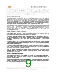
Temporary Sector Unprotect Mode
EN29F002A allows protected sectors to be temporarily unprotected for making changes to data
stored in a protected sector in system (n/a for EN29F002AN). To activate the temporary sector
unprotect, the
pin must be set to a high voltage of VID (11V). In this mode, protected sectors
RESET
can be programmed or erased by selecting the sector addresses. Once the high voltage, VID, is
removed from pin, all previously protected sectors will revert to their protected state.
RESET
RESET Hardware Reset Mode (not available on EN29F002AN)
Resetting the EN29F002A device is performed when the
pin is set to VIL and kept low for at
RESET
least 500ns. The internal state machine will be reset to the read mode. Any program/erase
operation in progress during hardware reset will be terminated and data may be corrupted.
If the
pin is tied to the system reset command, the device will be automatically reset to the
RESET
read mode and enable the system’s microprocessor to read the boot-up firmware from the FLASH
memory.
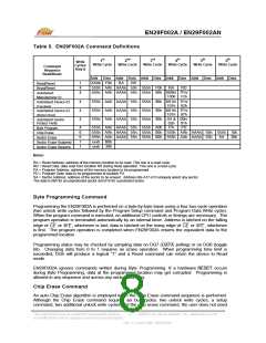
COMMAND DEFINITIONS
The operations of the EN29F002A are selected by one or more commands written into the
command register to perform Read/Reset Memory, Read ID, Read Sector Protection, Program,
Sector Erase, Chip Erase, Erase Suspend and Erase Resume. Commands are made up of data
sequences written at specific addresses via the command register. The sequences for the
specified operation are defined in the Command Table (Table 5). Incorrect addresses, incorrect
data values or improper sequences will reset the device to the read mode.
This Data Sheet may be revised by subsequent versions
©2003 Eon Silicon Solution, Inc., www.essi.com.tw
Rev. A, Issue Date: 2003/03/26
7
or modifications due to changes in technical specifications.

 EON [ EON SILICON SOLUTION INC. ]