EN29F002A / EN29F002AN
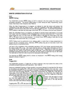
The flowchart for the Toggle Bit (DQ6) is shown in Flowchart 6. The Toggle Bit timing diagram is
shown in Figure 9.
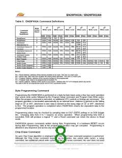
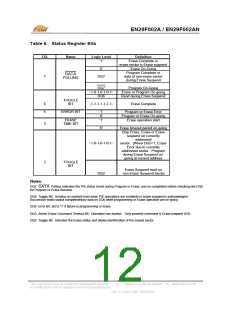
DQ5
Exceeded Timing Limits
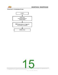
DQ5 will indicate if the program or erase time has exceeded the specified limits (internal pulse
count). Under these conditions DQ5 will produce a “1”. (The Toggle Bit (DQ6) should also be
checked at this time to make sure that the DQ5 is not a “1” due to the device having returned to read
mode.) This is a failure condition which indicates that the program or erase cycle was not
successfully completed.
function under this condition. Setting the
Polling (DQ7), Toggle Bit (DQ6) and Erase Toggle Bit (DQ2) still
to VIH will partially power down the device under those
CE
pins will control the output disable functions as described in Table 3.
DATA
conditions. The
and
WE
OE
The DQ5 failure condition will also appear if the user tries to program a “1” to a location that was
previously programmed to a “0”. In this case, the device goes into Hang or Error mode out and
never completes the Embedded Program Algorithm. Hence, the system never reads valid data on
DQ7 and DQ6 never stops toggling. Once the device exceeds the timing limits, DQ5 will indicate a
“1”. Please note that this is not a device failure condition since the device was used incorrectly. If
timing limits are exceeded, reset the device. (See Table 6)
DQ3
Sector Erase Command Timeout
This device does not support multiple sector erase commands. DQ3 will go high immediately after
the first 30h command (the sixth write cycle). Any extra 30h commands will be ignored (or taken as
a resume command if erase suspended).
DQ2
Erase Toggle Bit II
In the sector erase operation, DQ2 will toggle with
or
when a read is attempted within the
CE
OE
sector that is being erased. DQ2 will not toggle if the read address is not within the sector that is
selected to be erased. In the chip erase operation, however, DQ2 will toggle with
or
CE
OE
regardless of the address given by the user. This is because all sectors are to be erased. (See
Table 6)
This Data Sheet may be revised by subsequent versions
or modifications due to changes in technical specifications.
©2003 Eon Silicon Solution, Inc., www.essi.com.tw
11
Rev. A, Issue Date: 2003/03/26

 EON [ EON SILICON SOLUTION INC. ]