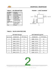
EN29F002A / EN29F002AN
USER MODE DEFINITIONS
Reset Mode
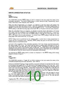
EN29F002A features a Reset mode that resets the program and erase operation immediately to
read mode. If reset (
= L) is executed when program or erase operation were in progress, the
RESET
program or erase which was terminated should be repeated since data will be corrupted. This pin is
not available for EN29F002AN.
Standby Mode
The EN29F002A / EN29F002AN has a CMOS-compatible standby mode which reduces the current
to < 1µA (typical). It is placed in CMOS-compatible standby when
and the
pins are at
RESET
CE
VCC ± 0.5 V (
pin only, for EN29F002AN). The device also has a TTL-compatible standby mode
CE
which reduces the maximum VCC current to < 1mA. It is placed in TTL-compatible standby when
CE
pin
and
pins are at VIH. Another method of entering standby mode uses only the
RESET
RESET
(n/a for EN29F002AN). When
pin is at VSS ± 0.3V, the device enters CMOS-compatible
RESET
standby with current typically reduced to < 1 µA. When
compatible standby with current reduced to < 1mA. When in standby modes, the outputs are in a
pin is at VIL, the device enters TTL-
RESET
high-impedance state independent of the
input.
OE
Read Mode
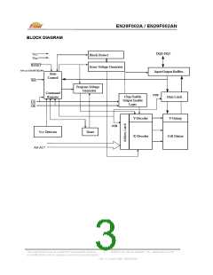
The EN29F002A / EN29F002AN has two control functions which must be satisfied in order to obtain
data at the outputs. Chip Enable ( ) is the power control and should be used for device selection.
CE
) is the output control and should be used to gate data to the output pins,
Output Enable (
OE
provided the device is selected. Read is selected when both
and
pins are held at VIL with
OE
CE
the
pin held at VIH. Address access time (tACC) is equal to the delay from stable addresses to
W E
valid output data. Assuming that addresses are stable, chip enable access time (tCE) is equal to the
delay from stable to valid data at output pins. Data is available at the outputs after output
CE
enable access time (tOE) from the falling edge of
, assuming the
has been LOW and
CE
OE
addresses have been stable for at least tACC - tOE.
Output Disable Mode
When the
or
pin is at a logic high level (VIH), the output from the EN29F002A /
OE
CE
EN29F002AN is disabled. The output pins are placed in a high impedance state.
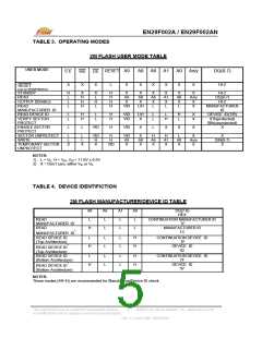
Auto Select Identification Mode
The manufacturer and device type can be identified by hardware or software operations. This mode
allows applications or programming equipment automatically matching the device with its
corresponding interface characteristics.
To activate the Auto Select Identification mode, the programming equipment must force 11.0 V ±
0.5V on address line A9 of the EN29F002AT/B. Two identifier bytes can then be sequenced from the
device outputs by toggling address lines A0 and A8 from VIL to VIH.
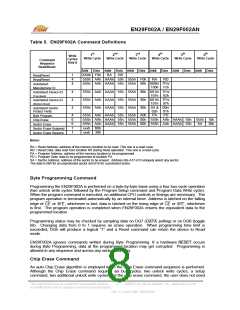
The manufacturer and device identification may also be read via the command register. By following
the command sequence referenced in the Command Definition Table (Table 5). This method is
desirable for in-system identification (using only + 5.0V).
When A0 = A1 = A6 = VIL and by toggling A8 from VIL to VIH, the Manufacturer ID can be read as Eon
= 7F, 1C (hex) to identify EON . When A0 = VIH, A1 = A6 = VIL, and by toggling A8 from VIL to VIH,
This Data Sheet may be revised by subsequent versions
©2003 Eon Silicon Solution, Inc., www.essi.com.tw
Rev. A, Issue Date: 2003/03/26
6
or modifications due to changes in technical specifications.

 EON [ EON SILICON SOLUTION INC. ]