EM78P341N/342N/343N
8-Bit Microprocessor with OTP ROM
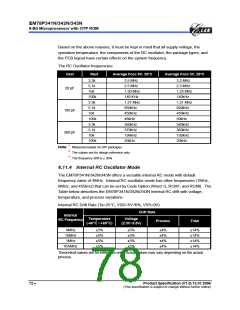
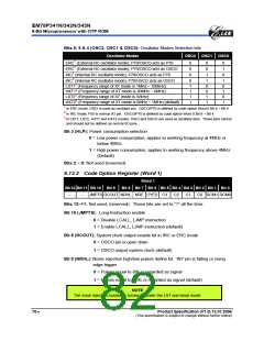
Bits 6, 5 & 4 (OSC2, OSC1 & OSC0): Oscillator Modes Selection bits
Oscillator Modes
OSC2 OSC1 OSC0
ERC1 (External RC oscillator mode); P70/OSCO acts as P70
ERC1 (External RC oscillator mode); P70/OSCO acts as OSCO
IRC2 (Internal RC oscillator mode); P70/OSCO acts as P70
0
0
0
0
0
1
0
1
0
IRC2 (Internal RC oscillator mode); P70/OSCO acts as OSCO
LXT13 (Frequency range of XT mode is 1MHz ~ 100kHz)
HXT13 (Frequency range of XT mode is 20MHz ~ 6MHz)
LXT23 (Frequency range of XT mode is 32kHz)
0
1
1
1
1
1
0
0
1
1
1
0
1
0
1
HXT23 (Frequency range of XT mode is 6MHz ~ 1MHz) (default)
1 In ERC mode, OSCI is used as oscillator pin. OSCO/P70 is defined by code option Word 0 Bit 6 ~ Bit 4.
2 In IRC mode, P55 is normal I/O pin. OSCO/P70 is defined by code option Word 0 Bit 6 ~ Bit 4.
3 In LXT1, LXT2, HXT1 and HXT2 modes; OSCI and OSCO are used as oscillator pins. These pins cannot
and should not be defined as normal I/O pins.
Bit 3 (HLP): Power consumption selection
0 = Low power consumption, applies to working frequency at 4MHz or
below 4MHz
1 = High power consumption, applies to working frequency above 4MHz
(Default)
Bits 2 ~ 0: Not used (reserved)
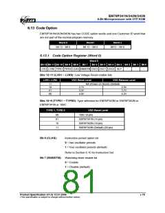
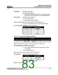
6.13.2 Code Option Register (Word 1)
Word 1
Bit 12 Bit 11 Bit 10 Bit 9
Bit 8 Bit 7 Bit 6 Bit 5 Bit 4 Bit 3 Bit 2 Bit 1 Bit 0
C2 C1 C0 RCM1 RCM0
–
–
JMPTS RCOUT NRHL NRE CYES C3
Bits 12~11: Not used, (reserved). These bits are set to “1” all the time.
Bit 10 (JMPTS): Long Instruction enable
0 = Disable LCALL, LJMP instruction
1 = Enable LCALL, LJMP instruction.(default)
Bit 8 (RCOUT): System clock output enable bit in IRC or ERC mode
0 = OSCO pin is open drain
1 = OSCO output system clock (default)
Bit 8 (NRHL): Noise rejection high/low pulses define bit. INT pin is falling or rising
edge trigger
0 = Pulses equal to 8/fc is regarded as signal
1 = Pulses equal to 32/fc is regarded as signal (default)
NOTE
The noise rejection function is turned off under the LXT and sleep mode.
76 •
Product Specification (V1.0) 12.01.2006
(This specification is subject to change without further notice)

 ELAN [ ELAN MICROELECTRONICS CORP ]