EM78P258N
8-Bit Microprocessor with OTP ROM
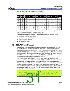
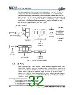
The watchdog timer is a free running on-chip RC oscillator. The WDT will keep on
running even when the oscillator driver has been turned off (i.e., in sleep mode).
During normal operation or sleep mode, a WDT time-out (if enabled) will cause the
device to reset. The WDT can be enabled or disabled at any time during normal mode
through software programming. Refer to WDTE bit of IOCE0 register (Section 6.2.10
IOCE0 (WDT Control & Interrupt Mask Registers 2). With no prescaler, the WDT
time-out period is approximately 18ms1 or or 4.5ms2.
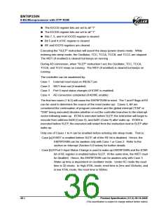
CLK (Fosc/2 or Fosc/4)
Data Bus
TCC (R1)
0
1
8-Bit Counter (IOCC1)
MUX
SYNC
2 cycles
TCC Pin
8 to 1 MUX
Prescaler
TE (CONT)
TCC overflow
interrupt
TS (CONT)
PSR2~0
(CONT)
WDT
8-Bit counter
8 to 1 MUX
Prescaler
WDTE
(IOCE0)
PSW2~0
(IOCE0)
WDT Time out
Fig. 6-1 TCC and WDT Block Diagram
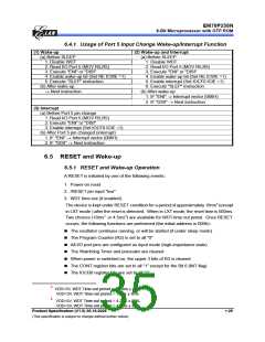
6.4 I/O Ports
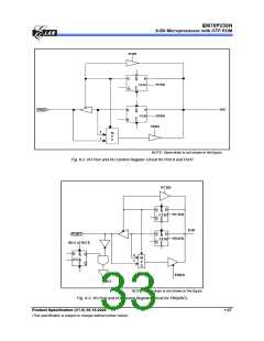
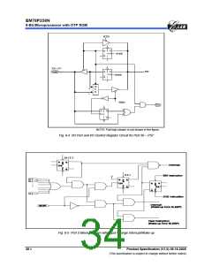
The I/O registers (Port 5, Port 6, and Port 7) are bi-directional tri-state I/O ports. Port 5
is pulled-high and pulled-down internally by software. Likewise, P6 has its open-drain
output through software. Port 5 features an input status changed interrupt (or wake-up)
function. Each I/O pin can be defined as "input" or "output" pin by the I/O control
register (IOC5 ~ IOC7). The I/O registers and I/O control registers are both readable
and writable. The I/O interface circuits for Port 5, Port 6, and Port7 are illustrated in
Figures 6-2, 6-3, 6-4, & 6-5 (see next page).
1
VDD=5V, WDT Time-out period = 16.5ms ± 30%.
VDD=3V, WDT Time-out period = 18ms ± 30%.
2
VDD=5V, WDT time-out period = 4.2ms ± 30%.
VDD=3V, WDT time-out period = 4.5ms ± 30%.
26 •
Product Specification (V1.0) 06.16.2005
(This specification is subject to change without further notice)

 ELAN [ ELAN MICROELECTRONICS CORP ]