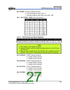
EM78P258N
8-Bit Microprocessor with OTP ROM
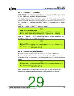
6.2.19 IOCC1 (TCC Prescaler Counter)
TCC prescaler counter can be read and written:
TCC
Rate
PST2 PST1 PST0 Bit 7 Bit 6 Bit 5 Bit 4 Bit 3 Bit 2 Bit 1 Bit 0
0
0
0
0
1
1
1
1
0
0
1
1
0
0
1
1
0
1
0
1
0
1
0
1
-
-
-
-
-
-
-
-
-
-
-
V
V
V
V
V
V
V
V
1:2
1:4
-
-
V
V
V
V
V
V
V
-
-
-
-
-
V
V
V
V
V
V
1:8
-
-
-
-
V
V
V
V
V
1:16
1:32
1:64
1:128
1:256
-
-
-
V
V
V
V
-
-
V
V
V
-
V
V
V
V = valid value
The TCC prescaler counter is assigned to TCC (R1).
The contents of the IOCC1 register is cleared when one of the following occurs:
ꢀ
ꢀ
ꢀ
ꢀ
a value is written to TCC register
a value is written to TCC prescaler bits (Bit3,2,1,0 of CONT)
power on reset, /RESET
WDT time out reset
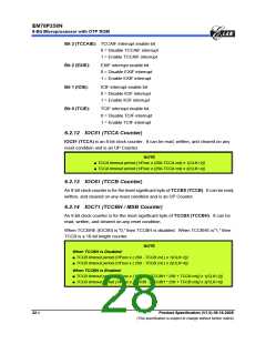
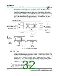
6.3 TCC/WDT and Prescaler
There are two 8-bit counters available as prescalers that can be extended to 16-bit
counter for the TCC and WDT respectively. The PST2 ~ PST0 bits of the CONT
register are used to determine the ratio of the TCC prescaler, and the PWR2 ~ PWR0
bits of the IOCE0 register are used to determine the prescaler of WDT. The prescaler
counter is cleared by the instructions each time such instructions are written into TCC.
The WDT and prescaler will be cleared by the “WDTC” and “SLEP” instructions. Fig.
6-1 (next page) depicts the block diagram of TCC/WDT.
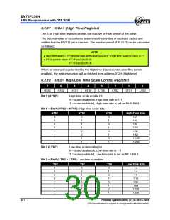
TCC (R1) is an 8-bit timer/counter. The TCC clock source can be internal clock or
external signal input (edge selectable from the TCC pin). If TCC signal source is from
internal clock, TCC will increase by 1 at every instruction cycle (without prescaler).
Referring to Fig. 6-1, CLK=Fosc/2 or CLK=Fosc/4 is dependent to the CODE Option bit
<CLKS>. CLK=Fosc/2 if the CLKS bit is "0," and CLK=Fosc/4 if the CLKS bit is "1." If
TCC signal source is from external clock input, TCC will increase by 1 at every falling
edge or rising edge of the TCC pin. TCC pin input time length (kept in High or Low
level) must be greater than 1CLK.
NOTE
The internal TCC will stop running when sleep mode occurs. However, during AD
conversion, when TCC is set to “SLEP” instruction, if the ADWE bit of RE register is
enabled, the TCC will keep on running
Product Specification (V1.0) 06.16.2005
• 25
(This specification is subject to change without further notice)

 ELAN [ ELAN MICROELECTRONICS CORP ]