EM78P258N
8-Bit Microprocessor with OTP ROM
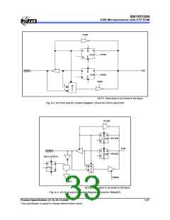
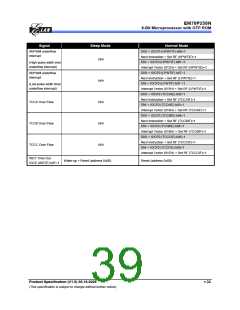
6.4.1 Usage of Port 5 Input Change Wake-up/Interrupt Function
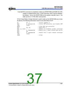
(1) Wake-up
(a) Before SLEEP
1. Disable WDT
(2) Wake-up and Interrupt
(a) Before SLEEP
1. Disable WDT
2. Read I/O Port 5 (MOV R5,R5)
3. Execute "ENI" or "DISI"
4. Enable wake-up bit (Set RE ICWE =1)
5. Execute "SLEP" instruction
(b) After wake-up
2. Read I/O Port 5 (MOV R5,R5)
3. Execute "ENI" or "DISI"
4. Enable wake-up bit (Set RE ICWE =1)
5. Enable interrupt (Set IOCF0 ICIE =1)
6. Execute "SLEP" instruction
(b) After wake-up
→ Next instruction
1. IF "ENI" → Interrupt vector (006H)
2. IF "DISI" → Next instruction
(3) Interrupt
(a) Before Port 5 pin change
1. Read I/O Port 5 (MOV R5,R5)
2. Execute "ENI" or "DISI"
3. Enable interrupt (Set IOCF0 ICIE =1)
(b) After Port 5 pin changed (interrupt)
1. IF "ENI" → Interrupt vector (006H)
2. IF "DISI" → Next instruction
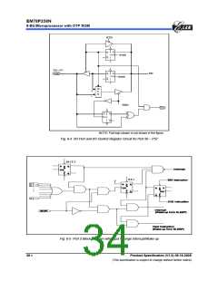
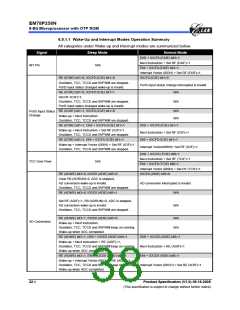
6.5 RESET and Wake-up
6.5.1 RESET and Wake-up Operation
A RESET is initiated by one of the following events:
1. Power-on reset
2. /RESET pin input "low"
3. WDT time-out (if enabled).
The device is kept under RESET condition for a period of approximately 18ms3 (except
in LXT mode ) after the reset is detected. When in LXT mode, the reset time is 500ms.
Two choices (18ms3 or 4.5ms4) are available for WDT-time out period. Once RESET
occurs, the following functions are performed (the initial address is 000h):
ꢀ The oscillator continues running, or will be started (if under sleep mode)
ꢀ The Program Counter (R2) is set to all "0"
ꢀ All I/O port pins are configured as input mode (high-impedance state)
ꢀ The Watchdog Timer and prescaler are cleared
ꢀ When power is switched on, the upper 3 bits of R3 is cleared
ꢀ The CONT register bits are set to all "1" except for the Bit 6 (INT flag)
ꢀ The IOCB0 register bits are set to all "1"
3
4
VDD=5V, WDT Time-out period = 16.5ms ± 30%.
VDD=3V, WDT Time-out period = 18ms ± 30%.
VDD=5V, WDT Time-out period = 4.2ms ± 30%.
VDD=3V, WDT Time-out period = 4.5ms ± 30%.
Product Specification (V1.0) 06.16.2005
• 29
(This specification is subject to change without further notice)

 ELAN [ ELAN MICROELECTRONICS CORP ]