EM78P258N
8-Bit Microprocessor with OTP ROM
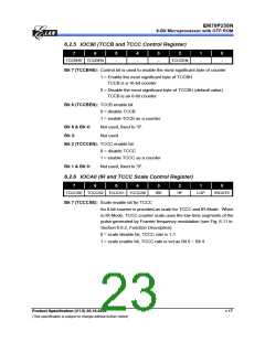
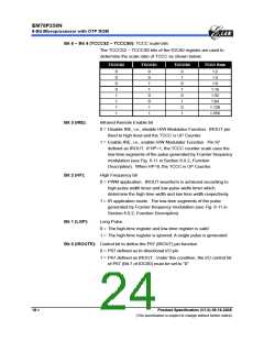
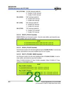
Bit 6 ~ Bit 4 (TCCCS2 ~ TCCCS0): TCCC scale bits
The TCCCS2 ~ TCCCS0 bits of the IOCA0 register are used to
determine the scale ratio of TCCC as shown below:
TCCCS2
TCCCS1
TCCCS0
TCCC Rate
0
0
0
0
1
1
1
1
0
0
1
1
0
0
1
1
0
1
0
1
0
1
0
1
1:2
1:4
1:8
1:16
1:32
1:64
1:128
1:256
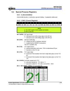
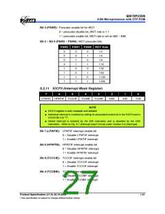
Bit 3 (IRE):
Infrared Remote Enable bit
0 = Disable IRE, i.e., disable H/W Modulator Function. IROUT pin
fixed to high level and the TCCC is UP Counter.
1 = Enable IRE, i.e., enable H/W Modulator Function. Pin 67
defined as IROUT. If HP=1, the TCCC counter scale uses the
low-time segments of the pulse generated by Fcarrier frequency
modulation (see Fig. 6-11 in Section 6.8.2, Function
Description). When HP=0, the TCCC is UP Counter.
Bit 2 (HF):
High Frequency bit
0 = PWM application. IROUT waveform is achieved according to
high-pulse width timer and low-pulse width timer which
determine the high time width and low time width respectively
1 = IR application mode. The low-time segments of the pulse
generated by Fcarrier frequency modulation (see Fig. 6-11 in
Section 6.8.2, Function Description)
Bit 1 (LGP):
Long Pulse.
0 = The high-time register and low-time register is valid
1 = The high-time register is ignored. A single pulse is generated
Bit 0 (IROUTE): Control bit to define the P67 (IROUT) pin function
0 = P67 defined as bi-directional I/O pin
1 = P67 defined as IROUT. Under this condition, the I/O control bit
of P67 (Bit 7 of IOC60) must be set to “0”
18 •
Product Specification (V1.0) 06.16.2005
(This specification is subject to change without further notice)

 ELAN [ ELAN MICROELECTRONICS CORP ]