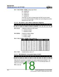
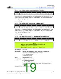
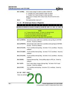
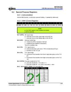
欢迎访问ic37.com |
会员登录 免费注册
发布采购

EM78P259NSO14J 参数 Datasheet PDF下载

EM78P259NSO14J图片预览
型号: EM78P259NSO14J
PDF下载: 下载PDF文件 查看货源
内容描述: [EM78Q153SN EM78P153SP EM78P153SN EM78156EH EM78156EP EM78156EM EM78156EKM EM78Q156ELP EM78Q156ELM EM78Q156ELKM EM78P156ELP EM78P156ELM EM78P156ELKM EM78P156NP EM78P156NM EM78447SH EM78447SAP EM78447SAM EM78447SAS EM78447SBP EM78447SBWM EM78Q447SH EM78Q447SAP EM78Q447SAM EM78Q447SBP EM78Q447SBWM EM78P447SAP EM78P447SAM EM78P447SAS EM78P447SBP EM78P447SBWM EM78Q257 EM78Q257AP EM78Q257AM EM78Q257BP EM78Q257BM EM78P257AP EM78P257AM EM78P257BP EM78P257BM EM78451H EM78451P EM78451AQ EM]
分类和应用:
文件页数/大小: 81 页 / 2574 K
品牌: ELAN [ ELAN MICROELECTRONICS CORP ]
 浏览型号EM78P259NSO14J的Datasheet PDF文件第18页浏览型号EM78P259NSO14J的Datasheet PDF文件第19页浏览型号EM78P259NSO14J的Datasheet PDF文件第20页浏览型号EM78P259NSO14J的Datasheet PDF文件第21页浏览型号EM78P259NSO14J的Datasheet PDF文件第23页浏览型号EM78P259NSO14J的Datasheet PDF文件第24页浏览型号EM78P259NSO14J的Datasheet PDF文件第25页浏览型号EM78P259NSO14J的Datasheet PDF文件第26页  
EM78P258N  
8-Bit Microprocessor with OTP ROM  
NOTE  
Tcc timeout period [1/Fosc x prescaler x 256(Tcc cnt) x 1(CLK=2)]  
Tcc timeout period [1/Fosc x prescaler x 256(Tcc cnt) x 2(CLK=4)]  
6.2.3 IOC50 ~ IOC70 (I/O Port Control Register)  
"1" puts the relative I/O pin into high impedance, while "0" defines the relative I/O  
pin as output.  
Only the lower 6 bits of IOC50 can be defined.  
Only the bit1, 2, 6 and, 7 of IOC60 can be defined.  
Only the lower 1 bits of IOC70 can be defined, the others bits are not available.  
IOC50, IOC60, and IOC70 registers are all readable and writable  
6.2.4 IOC80 (TCCA Control Register)  
7
6
5
4
3
2
1
0
-
-
-
TCCAEN TCCATS TCCATE  
NOTE  
Bit4 ~ 0 of IOC80 register is both readable and writable.  
Bit5 of IOC80 register is readable only.  
Bit 7 ~ Bit 5:  
Bit 4 & Bit 3:  
Not used  
Not used, fixed to “0”.  
Bit 2 (TCCAEN): TCCA enable bit  
0 = disable TCCA  
1 = enable TCCA as a counter  
TCCA signal source  
Bit 1 (TCCATS):  
Bit 0 (TCCATE):  
0 =: internal instruction cycle clock. P61 is a bi-directional I/O pin.  
1 = transit through the TCCA pin  
TCCA signal edge  
0 = increment if transition from low to high takes place on the  
TCCA pin  
1 = increment if transition from high to low takes place on the  
TCCA pin  
16 •  
Product Specification (V1.0) 06.16.2005  
(This specification is subject to change without further notice)  
 复制成功!