DA14580
FINAL
Bluetooth Low Energy 4.2 SoC
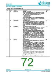
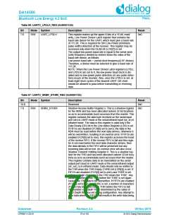
Table 96: UART2_LPDLH_REG (0x50001124)
Bit
Mode Symbol
R/W UART_LPDLH
Description
Reset
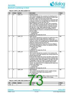
7:0
This register makes up the upper 8-bits of a 16-bit, read/
write, Low Power Divisor Latch register that contains the
baud rate divisor for the UART, which must give a baud rate
of 115.2K. This is required for SIR Low Power (minimum
pulse width) detection at the receiver. This register may be
accessed only when the DLAB bit (LCR[7]) is set.
The output low-power baud rate is equal to the serial clock
(sclk) frequency divided by sixteen times the value of the
baud rate divisor, as follows:
0x0
Low power baud rate = (serial clock frequency)/(16* divisor)
Therefore, a divisor must be selected to give a baud rate of
115.2K.
NOTE: When the Low Power Divisor Latch registers (LPDLL
and LPDLH) are set to 0, the low-power baud clock is dis-
abled and no low-power pulse detection (or any pulse detec-
tion) occurs at the receiver. Also, once the LPDLH is set, at
least eight clock cycles of the slowest UART Ctrl clock
should be allowed to pass before transmitting or receiving
data.
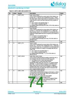
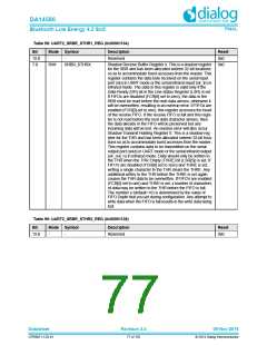
Table 97: UART2_SRBR_STHR0_REG (0x50001130)
Bit
Mode Symbol
Description
Reset
0x0
15:8
7:0
-
-
Reserved
R/W
SRBR_STHRX
Shadow Receive Buffer Register x: This is a shadow register
for the RBR and has been allocated sixteen 32-bit locations
so as to accommodate burst accesses from the master. This
register contains the data byte received on the serial input
port (sin) in UART mode or the serial infrared input (sir_in) in
infrared mode. The data in this register is valid only if the
Data Ready (DR) bit in the Line status Register (LSR) is set.
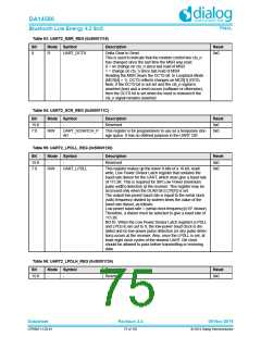
If FIFOs are disabled (FCR[0] set to zero), the data in the
RBR must be read before the next data arrives, otherwise it
will be overwritten, resulting in an overrun error. If FIFOs are
enabled (FCR[0] set to one), this register accesses the head
of the receive FIFO. If the receive FIFO is full and this regis-
ter is not read before the next data character arrives, then
the data already in the FIFO will be preserved but any
incoming data will be lost. An overrun error will also occur.
Shadow Transmit Holding Register 0: This is a shadow reg-
ister for the THR and has been allocated sixteen 32-bit loca-
tions so as to accommodate burst accesses from the master.
This register contains data to be transmitted on the serial
output port (sout) in UART mode or the serial infrared output
(sir_out_n) in infrared mode. Data should only be written to
the THR when the THR Empty (THRE) bit (LSR[5]) is set. If
FIFO's are disabled (FCR[0] set to zero) and THRE is set,
writing a single character to the THR clears the THRE. Any
additional writes to the THR before the THRE is set again
causes the THR data to be overwritten. If FIFO's are enabled
(FCR[0] set to one) and THRE is set, x number of characters
of data may be written to the THR before the FIFO is full.
The number x (default=16) is determined by the value of
FIFO Depth that you set during configuration. Any attempt to
write data when the FIFO is full results in the write data being
lost.
0x0
Datasheet
Revision 3.4
09-Nov-2016
CFR0011-120-01
76 of 155
© 2014 Dialog Semiconductor

 DIALOG [ Dialog Semiconductor ]