DA14580
FINAL
Bluetooth Low Energy 4.2 SoC
input/output characteristics'.
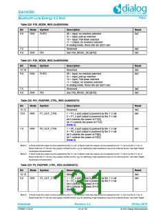
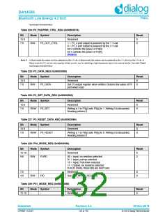
Table 224: P3_PADPWR_CTRL_REG (0x50003074)
Bit
Mode Symbol
Description
Reset
15:8
7:0
-
-
Reserved
0
0
R/W
P3_OUT_CTRL
1 = P3_x port output is powered by the 1 V rail
0 = P3_x port output is powered by the 3 V rail
bit 0 controls the power of P3[0],
bit 7 controls the power of P3[7],
(Note 6)
Note 6: In Buck mode the output must be powered by the 3 V rail. In Boost mode the outputs can be powered by the 1 V rail or by the 3 V rail. In
Boost mode the 3 V rail can only supply a limited current, e.g. for switching a high-impedance input of an external device. See table 'Digital
input/output characteristics'.
Table 225: P3_DATA_REG (0x50003080)
Bit
Mode Symbol
Description
Reset
15:8
7:0
-
-
Reserved
0
0
R/W
P3_DATA
Set P3 output register when written; Returns the value of P3
port when read
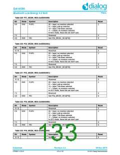
Table 226: P3_SET_DATA_REG (0x50003082)
Bit
Mode Symbol
Description
Reset
15:8
7:0
-
-
Reserved
0
0
R0/W
P3_SET
Writing a 1 to P3[y] sets P3[y] to 1. Writing 0 is discarded;
Reading returns 0
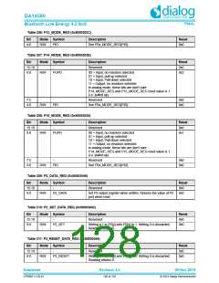
Table 227: P3_RESET_DATA_REG (0x50003084)
Bit
Mode Symbol
Description
Reset
15:8
7:0
-
-
Reserved
0
0
R0/W
P3_RESET
Writing a 1 to P0[y] sets P0[y] to 0. Writing 0 is discarded;
Reading returns 0
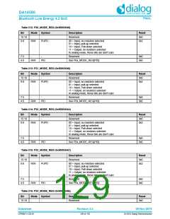
Table 228: P30_MODE_REG (0x50003086)
Bit
Mode Symbol
Description
Reset
15:10
9:8
-
-
Reserved
0
2
R/W
PUPD
00 = Input, no resistors selected
01 = Input, pull-up selected
10 = Input, Pull-down selected
11 = Output, no resistors selected
In ADC mode, these bits are don't care
7:5
4:0
-
-
Reserved
0
0
R/W
PID
See P0x_MODE_REG[PID]
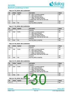
Table 229: P31_MODE_REG (0x50003088)
Bit
Mode Symbol
Description
Reset
15:10
-
-
Reserved
0
Datasheet
Revision 3.4
09-Nov-2016
CFR0011-120-01
132 of 155
© 2014 Dialog Semiconductor

 DIALOG [ Dialog Semiconductor ]