will cause the next valid ARINC word received to
overwrite the existing data in FIFO location 32.
(/HF2) pin is intended to act as an interrupt flag to the
systems external microprocessor, allowing a 16 word data
retrieval routine to be performed, without the user needing
to continually poll the status register bits.
A FIFO half full flag /HF1 (/HF2) goes low if the FIFO
contains 16 or more received ARINC words. The /HF1
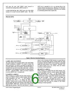
RECEIVERS
Figure 1 Receiver Function Diagram
write to all 16 location of label memory to ensure that no
previous unwanted label memory residual affect the label
recognition. Note that ARINC word reception is suspended
during the label memory write sequence. Therefore, CR1
of control register has to be written with zero before
returning to normal operation.
LABEL RECOGNITION
The chip compares the incoming label to the stored labels
if label recognition is enabled. If a match is found, the
data is processed. If a match is not found, no indicators of
receiving ARINC data are presented. Note that 00 (Hex) is
treated in the same way as any other label value. Label bit
significance is not changed by the status of control register
bit CR15. Label bits BD00 – BD07 are always compared
to receive ARINC bits 1- 8 respectively.
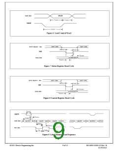
READING LABELS
When writing to, or reading from the label memory, SEL
must be set HIGH. Write to control register with Enable
Label Read/Write (set CR1 = 1) and Disable Label
recognition (set CR2,3 = 0) during the label read sequence.
Then the next 16 data reads of the selected receiver (/EN
taken low) are labels. /EN1 is used to read labels for
receiver 1, and /EN2 to read labels for receiver 2. Label
data is presented on BD00 – BD07. All 16 locations should
be accessed, and CR1 must be written to zero before
returning to normal operation.
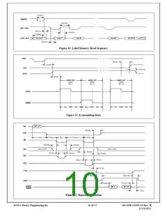
LOADING LABELS
When writing to, or reading from the label memory, SEL
must be set HIGH. Write to control register with Enable
Label Read/Write (set CR1 = 1) and Disable Label
recognition (set CR2,3 = 0) during the label write
sequence. Then the next 16 writes of data (/PL pulsed low)
load the label data into each location of the label memory
from the BD00 – BD07 pins. The /PL1 pin is used to write
label data for receiver 1 and /PL2 for receiver 2. Always
©2015 Device Engineering Inc.
6 of 15
DS-MW-01084-02 Rev. H
11/24/2015

 DEIAZ [ Device Engineering Incorporated ]