FUNCTIONAL DESCRIPTION
RECEIVER
The receiver signals (DI(A) and DI(B)) are differential,
bipolar, return-to-zero logic signals. The ARINC channels
can be connected directly to the receiver with no external
components.
ANALOG FRONT END (AFE) WITH LIGHTNING
PROTECTION. The AFE implements the analog detection
portion of the receiver circuit. The ARINC 429
characteristic describes RX detection levels as follows.
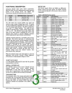
Table 1: DEI1084 Pin Description
STATE
ONE
NULL
ZERO
DIFFERENTIAL VOLTAGE
+6.5V to +13V
SIGNAL
VDD
FUNCTION
POWER
INPUT
DESCRIPTION
Power Input: +3V or +5V .
ARINC receiver 1 positive input.
ARINC receiver 1 negative input.
ARINC receiver 2 positive input.
ARINC receiver 2 negative input.
Receiver 1 data flag ready.
Receiver 1 FIFO full.
+2.5V to -2.5V
-6.5V to -13V
RIN1A
RIN1B
RIN2A
RIN1B
/DR1
INPUT
INPUT
The AFE detects the received ARINC line signal and
converts it into a stream of digital logic levels. It consists
of a pair of differential comparators per receiver capable of
±10V of common mode rejection. The AFE is powered by
an on chip 2.5V voltage regulator. This makes the part
capable of operating from a supply voltage ranging from
2.97V to 5.5V. The DEI1085 version parts bypass 10K
ohms of the input resistors, facilitating the use of 10K
external series resistors to provide lightning immunity
without impacting the input resistance specifications.
INPUT
OUTPUT
OUTPUT
OUTPUT
OUTPUT
OUTPUT
OUTPUT
INPUT
/FF1
/HF1
Receiver 1 FIFO half full.
/DR2
Receiver 2 data flag ready.
Receiver 2 FIFO full.
/FF2
/HF2
Receiver 2 FIFO half full.
SEL
Receiver data byte selection
(0 = BYTE 1) (1 = BYTE 2).
Data Bus control, enables receiver 1
data to output.
/EN1
/EN2
INPUT
INPUT
Lightning transient protection is provided at the receiver
input pins. The receiver input pins, in combination with
external 10K Ohm resistors, provide immunity to DO160
Level 3 Lightning Induced Transients. (These include the
600V peak damped sinusoid and 300V/150µs pulse). This
immunity is provided by the external 10K resistors
combined with the on-chip Zener diodes located within the
receiver input network. During a voltage transient, the
diodes shunt current to ground and drop most of the
transient voltage across the external resistors, thus
protecting the chip’s input pins.
Data Bus control, enables receiver 2
data to output.
BD[15:0]
GND
I/O
Data Bus.
POWER
INPUT
Power and signal ground.
/NFD
No frequency discrimination if low (pull
up)
/PL1
/PL2
INPUT
INPUT
Latch enable for byte 1 entered from
data bus to transmitter FIFO.
Latch enable for byte 2 entered from
data bus to transmitter FIFO. Must
follow /PL1.
When the internal resistor wire bond option is used, the
application must provide Transient Voltage Suppressor
(TVS) devices to limit transient voltage to ±120V.
TX/R
OUTPUT
Transmitter ready flag. Goes low when
ARINC word loaded into FIFO. Goes
high after transmission and FIFO empty.
Transmitter FIFO half full.
Transmitter FIFO full.
/HFT
OUTPUT
OUTPUT
OUTPUT
OUTPUT
OUTPUT
16 BIT DATA BUS
A 16 Bit parallel bi-directional tri-state data bus provides
communication to the host.
/FFT
429DO
/429DO
/TXSEL
“ONES” data output from transmitter.
“ZEROS” data output from transmitter.
Transmitter Speed Select Status. Hi =
High speed,
SERIAL INTERFACE
The DEI1084 consists of two receive channels and one
transmit channel. Each receive channel operates
independently of each other and the transmitter. The
receive data is asynchronous to the transmitter data and
can also be at a different data rate than the transmitter.
Lo = Low speed. Inverted control word
“TXSEL”.
ENTX
/CWSTR
/RSR
INPUT
INPUT
INPUT
Enable transmission.
Clock for control word register.
Read status register if SEL = 0, read
control register if SEL = 1 (pull up)
Master clock input.
TRANSMITTER
The transmitter clock is free running and in phase with the
transmitter data. The transmitter data (DO(A) and DO(B))
are TTL level signals. There are always at least 4 null bits
between data words. An external ARINC line driver is
required to interface the transmitter to the ARINC serial
data bus.
CLK
INPUT
TX CLK
OUTPUT
Transmitter clock equal to master clock
(CLK), divided by either 10 or 80.
Master reset.
/MR
INPUT
©2015 Device Engineering Inc.
3 of 15
DS-MW-01084-02 Rev. H
11/24/2015

 DEIAZ [ Device Engineering Incorporated ]