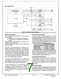
If the /NFD pin is HI, the device accepts signals that meet
these specifications and rejects signals outside the
tolerances. The way this is achieved is described below:
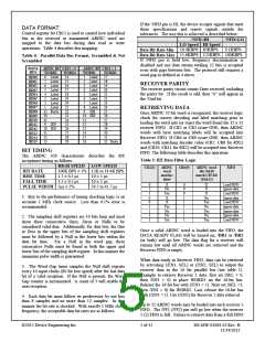
DATA FORMAT
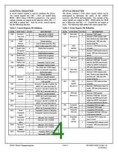
Control register bit CR15 is used to control how individual
bits in the received or transmitted ARINC word are
mapped to the data bus during data read or write
operations. Table 4 describes this mapping:
/NFD=HI
/NFD=LO
LO Speed HI Speed
10.4KBPS 83KBPS
15.6KBPS 125KBPS 500KBPS
0.1KBPS
Data Bit Rate Min
Data Bit Rate Max
Table 4: Parallel Data Bus Format, Scrambled & Not
Scrambled
If /NFD pin is held low, frequency discrimination is
disabled and any data stream totaling 32 bits is accepted
even with gaps between bits. The protocol still requires a
word gap as defined in 4 above.
DATA
BUS
ARINC BIT CR15 = 0
WORD1
ARINC BIT CR15 = 1
WORD2
14
15
16
17
18
19
20
21
22
23
24
25
26
27
28
29
WORD1
WORD2
8
7
6
5
4
3
2
1
Label
Label
Label
Label
Label
Label
Label
Label
1
2
3
4
5
6
7
8
9
Label
Label
Label
Label
Label
Label
Label
Label
SDI
17
18
19
20
21
22
23
24
BD00
BD01
BD02
BD03
BD04
BD05
BD06
BD07
BD08
BD09
BD10
BD11
BD12
BD13
BD14
BD15
RECEIVER PARITY
The receiver parity circuit counts Ones received, including
the parity bit. If the result is odd, then “0” will appear in
the 32nd bit.
RETRIEVING DATA
32 Parity
30
31
25
Once ARINC 32-bit word is recognized, the receiver logic
check for correct decoding and label matching prior to
loading the word into (or reject the word from) the 32 x 32
receiver FIFO. If CR2 or CR3 is/are ONE, then ARINC
words with have matching labels will be accepted into
Receiver FIFO. If CR6 or CR9 is/are ONE, then ARINC
words with matching decoder value (CR7, CR8 for RX1)
and (CR10, CR11 for RX2) will be accepted into Receiver
FIFO. The following table describes this operation:
10 SDI
26
11
12
13
14
15
16
27
28
29
30
9
SDI
10 SDI
11
12
13
31
32 Parity
BIT TIMING
The ARINC 429 characteristic describes the RX
acceptance timing as follows.
Table 5: RX Data Filter Logic
HIGH SPEED LOW SPEED
100K BPS ± 1% 12K to 14.4K BPS
CR2(3)
ARINC
word
matches
label
CR6(9)
ARINC word
bits 9&10
match CR7&8
(10&11)
FIFO
BIT RATE
1.5 ± 0.5 µs
1.5 ± 0.5 µs
5µs ± 5%
10 ± 5 µs
10 ± 5 µs
34.5 to 41.7 µs
RISE TIME
FALL TIME
PULSE WIDTH
0
1
1
0
0
1
1
1
1
X
No
Yes
X
0
0
0
1
1
1
1
1
1
X
X
X
No
Yes
No
Yes
No
Yes
Load FIFO
Ignore data
Load FIFO
Ignore data
Load FIFO
Ignore data
Ignore data
Ignore data
Load FIFO
1. Key to the performance of timing checking logic is an
accurate 1 MHz clock source. Less than 0.1% error is
recommended.
X
Yes
No
No
Yes
2. The sampling shift registers are 10 bits long and must
show three consecutive Ones, Zeros or Nulls to be
considered valid data. Additionally, for data bits, the One
or Zero in the upper bits of the sampling shift registers
must be followed by a Null in the lower bits within the
data bit time. For a Null in the word gap, three
consecutive Nulls must be found in both the upper and
lower bits of the sampling shift register. In this manner the
minimum pulse width is guaranteed.
Once a valid ARINC word is loaded into the FIFO, the
DATA READY FLAG will be turned on; /DR1 or /DR2
(or both) will go low. The data flag for a receiver will
remain low until all ARINC words are retrieved and the
Receiver FIFO is empty.
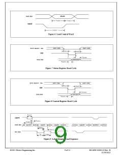
When data ready in Receiver FIFO, data can be retrieved
by activating (/EN1, SEL) or (/EN2, SEL) to output the
receiver data to the 16 bit parallel bus (see table 1).
Example to retrieve Receiver 1 data, first set (SEL = 0,
then /EN1 = 0) to place WORD1 on the 16-bit bus.
Release the 16-bit bus with (/EN1 = 1). Next set (SEL =1,
then /EN1 = 0) for WORD2. Last, release the 16-bit bus
with (/EN1 = 1). Use (/EN2) for Receiver 2 data retrieval.
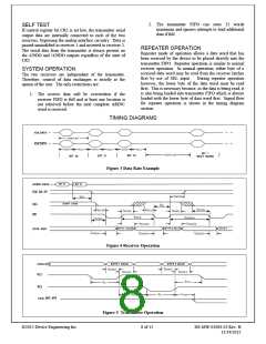
3. The Word Gap timer samples the Null shift register
every 10 input clocks (80 for low speed) after the last data
bit of a valid reception. If the Null is present, the Word
Gap counter is incremented. A count of 3 will enable the
next reception.
4. Each data bit must follow its predecessor by not less
than 8 samples and no more than 12 samples. In this
manner the bit rate is checked. With exactly 1 MHz clock
frequency, the acceptable data bit rates are as follows:
Up to 32 ARINC words may be loaded into each receiver’s
FIFO. The /FF1 (/FF2) pin will go low when the receiver
1 (2) FIFO is full. Failure to retrieve data from a full FIFO
©2015 Device Engineering Inc.
5 of 15
DS-MW-01084-02 Rev. H
11/24/2015

 DEIAZ [ Device Engineering Incorporated ]