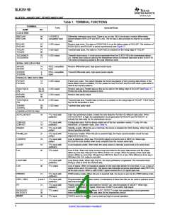
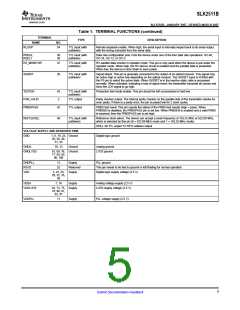
SLK2511B
www.ti.com
SLLS763B–JANUARY 2007–REVISED MARCH 2007
Table 6. Reference Clock Frequency
REFCLKSEL
REFERENCE CLOCK FREQUENCY
622.08 MHz
155.52 MHz
0
1
CLOCK AND DATA RECOVERY
The CDR unit of SLK2511B recovers the clock and data from the incoming data streams.
In the event of receive data loss, the PLL automatically locks to the local REFCLK to maintain frequency
stability. If the frequency of the data differs by more that 100 ppm with respect to the REFCLK frequency, the
LOL pin is asserted as a warning. Actual loss of lock occurs if the data frequency differs by more than 170 ppm.
MINIMUM TRANSITION DENSITY
The loop filter transfer function is optimized to enable the CDR to track ppm difference in the clocking and
tolerate the minimum transition density that can be received in a SONET data signal (±20 ppm). The transfer
function yields a typical capture time of 3500 bit times for random incoming NRZ data after the device is
powered up and achieves frequency locking.
The device tolerates up to 72 consecutive digits (CID) without sustaining an error.
JITTER TOLERANCE
Input jitter tolerance is defined as the peak-to-peak amplitude of sinusoidal jitter applied on the input signal that
causes the equivalent 1-dB optical/electrical power penalty. This refers to the ability of the device to withstand
input jitter without causing a recovered data error. The device has a jitter tolerance that exceeds the mask
shown in Figure 2 (GR-253 Figure 5-28)(1). This jitter tolerance is measured using a pseudorandom data pattern
of 231–1.
OC-N/STS-N
LEVEL
f0
(Hz)
F1
(Hz)
F2
(Hz)
F3
(kHz)
F4
(kHz)
A1
(Ulpp)
A2
(Ulpp)
A3
(Ulpp)
3
10
10
30
30
300
300
6.5
25
65
0.15
0.15
1.5
1.5
15
15
12
24
48
250
Not Specified
10
600
6000
100
1000
0.15
1.5
15
(1) The tolerance margin is 20% or more at all modulating frequencies when measured using the HP 7150A jitter analysis system on the
Texas Instruments provided EVM.
Figure 2. Input Jitter Tolerance
8
Submit Documentation Feedback

 DBLECTRO [ DB LECTRO INC ]