SLK2511B
www.ti.com
SLLS763B–JANUARY 2007–REVISED MARCH 2007
HIGH-SPEED ELECTRICAL INTERFACE
The high-speed serial I/O uses a PECL compatible interface. The line could be directly coupled or ac-coupled.
See Figure 10 and Figure 11 for configuration details. As shown in the figures, an on-chip 100-Ω termination
resistor is placed differentially at the receive end.
The PECL output also provide de-emphasis for compensating ac loss when driving a cable or PCB backplane
over long distance. The level of the de-emphasis is programmable via PRE1 and PRE2 pins. Users can use
software to control the strength of the de-emphasis to optimize the device for a specific system requirement.
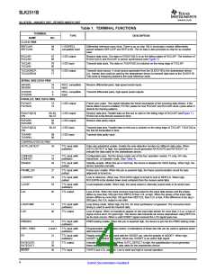
Table 5. Programmable De-Emphasis
PRE1
PRE2
DE-EMPHASIS LEVEL
(V(ODp)d/V(ODd)(1)– 1)
0
1
0
1
0
0
1
1
De-emphasis disabled
10%
20%
30%
(1) V(ODp): Differential voltage swing when there is a transition in the data stream.
V(ODd): Differential voltage swing when there is no transition in the data stream.
Figure 1. Output Differential Voltage Under De-Emphasis
LVDS PARALLEL DATA INTERFACE
The parallel data interface consists of a 4-bit parallel LVDS data and clock. The device conforms to OIF99.102
specification when operating at the OC-48 rate. When operating at lower serial rates the clock and data
frequency are scaled down accordingly, as indicated in Table 2. The parallel data TXDATA[0:3] is latched on the
rising edge of the TXCLK and then is sent to a data FIFO to resolve any phase difference between TXCLK and
REFCLK. If there is a FIFO overflow condition, the SPILL pin is set high. The FIFO resets itself to realign
between two clocks. The internal PLL for the clock synthesizer is locked to the REFCLK and it is used as the
timing to serialize the parallel data (except for the loop timing mode where the recovered clock is used). On the
receive side, RXDATA[0:3] is updated on the rising edge of RXCLK. Figure 7 and Figure 8 show the timing
diagram for the parallel interface.
The SLK2511B also has a built-in parity checker and generator for error detection of the LVDS interface. On the
transmit side, it accepts the parity bit, TXPARP/N, and performs the parity checking function for even parity. If an
error is detected, it pulses the PAR_VALID pin low for two clock cycles. On the receive side, the parity bit
RXPARP/N is generated for the downstream device for parity error checking.
Differential termination 100-Ω resistors are included on-chip between TXDATAP/N.
REFERENCE CLOCK
The device accepts either a 155.52-MHz or a 622.08-MHz clock. A clock select pin (REFCLKSEL) allows the
selection of the external reference clock frequency. The REFCLK input is compatible with the LVDS level and
also the 3.3-V LVPECL level using ac-coupling. A 100-Ω differential termination resistor is included on-chip, as
well as a dc biasing circuit (3 kΩ to VDD and 4.5 kΩ to GND) for the ac-coupled case. A high quality REFCLK
must be used on systems required to meet SONET/SDH standards. For non-SONET/SDH compliant systems,
loose tolerances may be used.
7
Submit Documentation Feedback

 DBLECTRO [ DB LECTRO INC ]