SLK2511B
www.ti.com
SLLS763B–JANUARY 2007–REVISED MARCH 2007
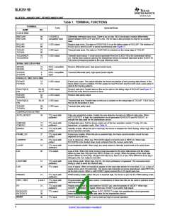
Table 1. TERMINAL FUNCTIONS (continued)
TERMINAL
NAME
RLOOP
TYPE
DESCRIPTION
NO.
54
TTL input (with
pulldown)
Remote loopback enable. When high, the serial input is internally looped back to its serial output
with the timing extracted from the serial data.
RSEL0,
RSEL1
39
38
TTL input (with
pulldown)
Data rate configuration pins. Puts the device under one of the four data rate operations: OC-48,
OC-24, OC-12, or OC-3.
RX_MONITOR
47
TTL input (with
pulldown)
RX parallel data monitor in repeater mode. This pin is only used when the device is put under the
repeater mode. When high, the RX demux circuit is enabled and the parallel data is presented.
When low, the demux is shut down to save power.
SIGDET
20
TTL input (with
pulldown)
Signal detect. This pin is generally connected to the output of an optical receiver. This signal may
be active high or active low depending on the optical receiver. The SIGDET input is XORed with
the PS pin to select the active state. When SIGDET is in the inactive state, data is processed
normally. When activated, indicating a loss of signal event, the transmitter transmits all zeroes and
force the LOS signal to go high.
TESTEN
43
2
TTL input (with
pulldown)
Production test mode enable. This pin should be left unconnected or tied low.
PAR_VALID
PRBSPASS
TTL output
Parity checker output. The internal parity checker on the parallel side of the transmitter checks for
even parity. If there is a parity error, the pin is pulsed low for 2 clock cycles.
42
TTL output
PRBS test result. This pin reports the status of the PRBS test results (high = pass). When
PRBSEN is disabled, the PRBSPASS pin is set low. When PRBSEN is enabled and a valid PRBS
is received, then the PRBSPASS pin is set high.
REFCLKSEL
40
TTL input (with
pulldown)
Reference clock select. The device can accept a clock frequency of 155.52 MHz or 622.08 MHz,
which is selected by this pin (0 = 622.08-MHz mode and 1 = 155.52-MHz mode).
SPILL 49 TTL output TX FIFO collision output
VOLTAGE SUPPLY AND RESERVED PINS
GND
1, 6, 19, 23, Ground
26, 28, 30,
Digital logic ground
31, 33
GNDA
10, 13
Ground
Analog ground
LVDS ground
GNDLVDS
61, 69, 76, Ground
77, 89, 93,
96, 100
GNDPLL
RSVD
VDD
12
52
Supply
PLL ground
Reserved
Supply
This pin needs to be tied to ground or left floating for normal operation.
Digital logic supply voltage (2.5 V)
3, 22, 25,
29, 32, 35,
50
VDDA
7, 16
Supply
Analog voltage supply (2.5 V)
LVDS supply voltage (2.5 V)
VDDLVDS
62, 72, 75, Supply
78, 90, 91,
92, 97
VDDPLL
11
Supply
PLL voltage supply (2.5 V)
5
Submit Documentation Feedback

 DBLECTRO [ DB LECTRO INC ]