SLK2511B
www.ti.com
SLLS763B–JANUARY 2007–REVISED MARCH 2007
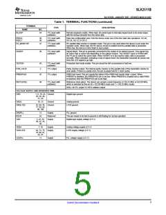
Table 1. TERMINAL FUNCTIONS
TERMINAL
TYPE
DESCRIPTION
NAME
NO.
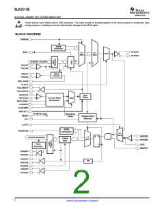
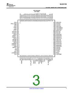
CLOCK PINS
REFCLKP,
REFCLKN
94
95
LVDS/PECL
compatible input
Differential reference input clock. There is an on-chip 100-Ω termination resistor differentially
placed between REFCLKP and REFCLKN. The dc bias is also provided on-chip for ac-coupled
case.
RXCLKP,
RXCLKN
67
68
LVDS output
LVDS input
LVDS output
Receive data clock. The data on RXDATA(0:3) is on the falling edges of RXCLKP. The interface of
RXDATA(0:3) and RXCLKP is source synchronous (see Figure 7).
TXCLKP,
TXCLKN
79
80
Transmit data clock. The data on TXDATA(0:3) is latched on the rising edge of TXCLKP.
TXCLKSRCP,
TXCLKSRCN
70
71
Transmit clock source. A clock source generated from the SLK2511B to the downstream device
(i.e., framer) that could be used by the downstream device to transmit data back to the SLK2511B.
This clock is frequency-locked to the local reference clock.
SERIAL SIDE DATA PINS
SRXDIP,
SRXDIN
14
15
PECL compatible
input
Receive differential pairs; high-speed serial inputs.
Transmit differential pairs; high-speed serial outputs.
STXDOP,
STXDON
9
8
PECL compatible
input
PARALLEL SIDE DATA PINS
FSYNCP,
FSYNCN
73
74
LVDS output
Frame sync pulse. This signal indicates the frame boundaries of the incoming data stream. If the
frame-detect circuit is enabled, FSYNC pulses for four RXCLKP and RXCLKN clock cycles when it
detects the framing patterns.
RXDATA[0:3]
P/N
66–63,
60–57
LVDS output
LVDS output
LVDS input
LVDS input
Receive data pins. Parallel data on this bus is valid on the falling edge of RXCLKP (seeFigure 7 ).
RXDATA0 is the first bit received in time.
RXPARP,
RXPARN
56
55
Receive data parity output
TXDATA[0:3]
P/N
88–81
Transmit data pins. Parallel data on this bus is clocked on the rising edge of TXCLKP. TXDATA0 is
the first bit transmitted in time.
TXPARP,
TXPARN
99
98
Transmit data parity input
CONTROL/STATUS PINS
AUTO_DETECT
34
TTL input (with
pulldown)
Data rate autodetect enable. Enable the auto-detection function for different data rates. When
AUTO_DETECT is high, the autodetection circuit generates RATEOUT0 and RATEOUT1 to
indicate the data rates for the downstream device.
CONFIG0,
CONFIG1
17
18
TTL input (with
pulldown)
Configuration pins. Put the device under one of the four operation modes: TX only, RX only,
transceiver, or repeater mode. (See Table 4)
ENABLE
FRAME_EN
LCKREFN
LLOOP
44
27
24
53
45
TTL input (with
pullup)
Standby enable. When this pin is held low, the device is disabled for IDDQ testing. When high, the
device operates normally.
TTL input (with
pullup)
Frame sync enable. When this pin is asserted high, the frame synchronization circuit for byte
alignment is turned on.
TTL input (with
pullup)
Lock to reference. When low, RXCLKP/N output is forced to lock to REFCLK. When high,
RXCLKP/N is the divided down clock extracted from the receive serial data.
TTL input (with
pulldown)
Local loopback enable. When high, the serial output is internally looped back to its serial input.
LOL
TTL output
Loss of lock. When the clock recovery loop has locked to the input data stream and the phase
differs by less than 100 ppm from REFCLK then LOL is high. When the phase of the input data
stream differs by more than 100 ppm from REFCLK, then LOL is low. If the difference is too big (>
500 ppm), the LOL output is not valid.
LOOPTIME
LOS
51
46
TTL input (with
pulldown)
Loop timing mode. When high, the PLL for clock synthesizer is bypassed. The recovered clock
timing is used to send the transmit data.
TTL output
Loss of signal. When no transitions appear on the input data stream for more than 2.3 µs, a loss of
signal occurs and LOS goes high. The device also transmits all zeroes downstream using REFCLK
as its clock source. When a valid SONET signal received the LOS signal goes low.
PRBSEN
41
TTL input (with
pulldown)
PRBS testing enable. When this pin is asserted high, the device is put into the PRBS testing mode.
PRE1, PRE2
PS
4 and 5
21
TTL input (with
pulldown)
Programmable de-emphasis control. Combinations of these two bits can be used to optimize serial
data transmission.
TTL input (with
pulldown)
Polarity select. This pin, used with the SIGDET pin, sets the polarity of SIGDET. When high,
SIGDET is an active low signal. When low, SIGDET is an active high signal.
RATEOUT0,
RATEOUT1
37
36
TTL output
Autorate detection outputs. When AUTO_DETECT is high, the autodetection circuit generates
these two bits to indicate the data rates for the downstream device.
RESET
48
TTL input
TXFIFO and LOL reset pin. Low is reset and high is normal operation.
4
Submit Documentation Feedback

 DBLECTRO [ DB LECTRO INC ]