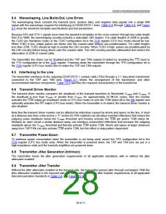
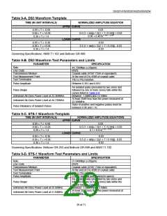
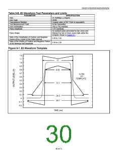
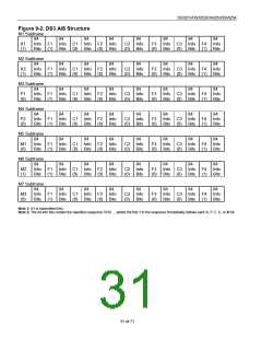
DS3251/DS3252/DS3253/DS3254
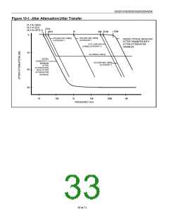
10. JITTER ATTENUATOR
Each LIU contains an on-board jitter attenuator that can be placed in the receive path or the transmit path or can
be disabled. The TJA and RJA pins (hardware mode) or the TCR:TJA and RCR:RJA control bits (CPU bus mode)
specify how the jitter attenuator is used. Setting TJA = RJA = 0 disables the jitter attenuator. To use the jitter
attenuator in the receive path, set RJA = 1 (with TJA = 0). To use it in the transmit path, set TJA = 1. Figure 10-1
shows the minimum jitter attenuation for the device when the jitter attenuator is enabled. Figure 10-1 also shows
the receive jitter transfer when the jitter attenuator is disabled.
The jitter attenuator consists of a narrowband PLL to retime the selected clock, a FIFO to buffer the associated
data while the clock is being retimed, and logic to prevent FIFO over/underflow in the presence of very large jitter
amplitudes. In hardware mode, only 16-bit and 32-bit FIFO depths are available. See Table 6-I. In CPU bus mode,
control bits TCR:JAL[1:0] set the FIFO depth to 16, 32, 64, or 128 bits.
The jitter attenuator requires a transmission-quality master clock (i.e., M20ppm frequency accuracy and low jitter).
When enabled in the receive path, the JA can obtain its master clock from the appropriate MCLK pin, from the
clock adapter block, or from the TCLK pin. When enabled in the transmit path, the JA can take its master clock
from the MCLK pin or from the clock adapter block, but not from the TCLK pin. The CDR block also uses the
selected master clock. See Section 12 for more information about master clocks and clock selection.
The JA has a loop bandwidth of master_clock T 2,058,874 (see corner frequencies in Figure 10-1). The JA
attenuates jitter at frequencies higher than the loop bandwidth, while allowing jitter (and wander) at lower
frequencies to pass through relatively unaffected.
In CPU bus mode the jitter attenuator indicates the fill status of its FIFO buffer in the JAFL (JA full) and JAEL (JA
empty) status bits in the SRL register. The JA sets the JAFL bit to indicate that its buffer is full. When the buffer
becomes full, the JA momentarily increases the frequency of the read clock by 6250 ppm to avoid buffer overflow
and consequent data loss. In a similar manner, the JA sets the JAEL bit to indicate that its buffer is empty. When
the buffer becomes empty, the JA momentarily decreases the frequency of the read clock by 6250 ppm to avoid
buffer underflow and consequent data errors. During these momentary frequency adjustments, jitter is passed
through the JA to avoid over/underflow. If the phase noise or frequency offset of the write clock is large enough to
cause the buffer to overflow or underflow, the JA sets both the JAFL bit and the JAEL bit to indicate that data errors
have occurred.
32 of 71

 DALLAS [ DALLAS SEMICONDUCTOR ]