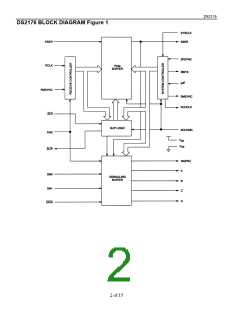
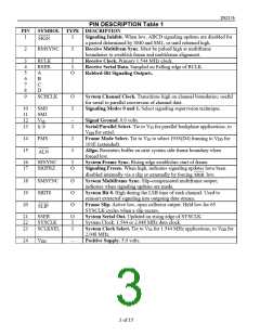
DS2176
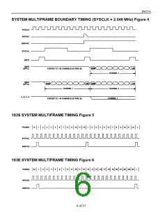
passed through the receive buffer and presented at SSER immediately after the rising edge of the system
side frame sync. The F–bit is dropped in 2.048 MHz applications and the MSB of channel 1 appears at
SSER one bit period after a rising edge at SFSYNC. SSER is forced to 1 in all channels greater than 24.
See Figures 3 and 4.
In 2.048 MHz applications (SCLKSEL=1), the PCM buffer control logic establishes slip criteria different
from that used in 1.544 MHz applications to compensate for the faster system-side read frequency.
PARALLEL COMPATIBILITY
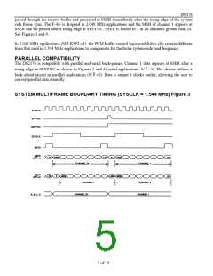
The DS2176 is compatible with parallel and serial back-planes. Channel 1 data appears at SSER after a
rising edge at SFSYNC as shown in Figures 3 and 4 (serial applications, S/ P =1). The device utilizes a
look–ahead circuit in parallel applications (S/ P =0). Data is output 8 clocks earlier, allowing the user to
convert parallel data eternally.
SYSTEM MULTIFRAME BOUNDARY TIMING (SYSCLK = 1.544 MHz) Figure 3
5 of 15

 DALLAS [ DALLAS SEMICONDUCTOR ]