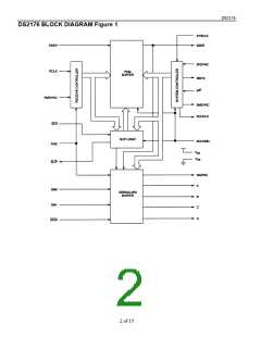
DS2176
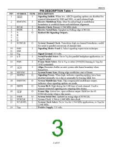
PIN DESCRIPTION Table 1
SYMBOL TYPE DESCRIPTION
PIN
1
I
Signaling Inhibit. When low, ABCD signaling updates are disabled for
a period determined by SM0 and SM1, or until returned high.
Receive Multifram Sync. Must be pulsed high at multiframe
boundaries to establish frame and multiframe alignment.
Receive Clock. Primary 1.544 MHz clock.
Receive Serial Data. Sampled on Falling edge of RCLK.
Robbed-Bit Signaling Outputs.
SIGN
2
RMSYNC
I
3
4
5
6
7
8
9
RCLK
RSER
A
B
C
D
I
I
O
SCHCLK
O
I
System Channel Clock. Transitions high on channel boundaries; useful
for serial to parallel conversion of channel data.
Signaling Modes 0 and 1. Select signaling supervision technique.
10
11
12
13
SM0
SM1
VSS
–
I
Signal Ground. 0.0 volts.
Serial/Parallel Select. Tie to VSS for parallel backplane applications, to
VDD for serial.
S/ P
14
15
FMS
ALN
I
I
Frame Mode Select. Tie to VSS to select 193S(D4) framing to VDD for
193E (extended).
Align. Recenters buffer on next system side frame boundary when
forced low.
16
17
SFSYNC
SIGFRZ
I
O
System Frame Sync. Rising edge establishes start of frame.
Signaling Freeze. When high, indicates signaling updates have been
disabled internally via a slip or externally by forcing SIGH low.
System Multiframe Sync. Slip-compensated multiframe output;
indicates when signaling updates are made.
System Bit 8. High during the LSB time of each channel. Used to
reinsert extracted signaling into outgoing data stream.
Frame Slip. Active low, open collector output. Held low for 65
SYSCLK cycles when a slip occurs.
18
19
20
SMSYNC
SBIT8
O
O
O
SLIP
21
22
23
SSER
SYSCLK
SCLKSEL
O
I
I
System Serial Out. Updated on rising edge of SYSCLK.
System Clock. 1.544 or 2.048 MHz data clock.
System Clock Select. Tie to VSS for 1.544 MHz applications, to VDD for
2.048 MHz.
24
VDD
–
Positive Supply. 5.0 volts.
3 of 15

 DALLAS [ DALLAS SEMICONDUCTOR ]