DS2154
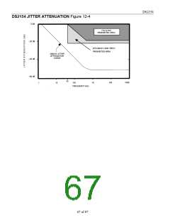
12.3 JITTER ATTENUATOR
The DS2154 contains an onboard jitter attenuator that can be set to a depth of either 32 or 128 bits via the
JABDS bit in the Line Interface Control Register (LICR). The 128-bit mode is used in applications
where large excursions of wander are expected. The 32-bit mode is used in delay sensitive applications.
The characteristics of the attenuation are shown in Figure 12-4. The jitter attenuator can be placed in
either the receive path or the transmit path by appropriately setting or clearing the JAS bit in the LICR.
Also, the jitter attenuator can be disabled (in effect, removed) by setting the DJA bit in the LICR. In order
for the jitter attenuator to operate properly, a 2.048 MHz clock (±50 ppm) must be applied at the MCLK
pin or a crystal with similar characteristics must be applied across the MCLK and XTALD pins. If a
crystal is applied across the MCLK and XTALD pins, then capacitors should be placed from each leg of
the crystal to ground as shown in Figure 12-1. Onboard circuitry adjusts either the recovered clock from
the clock/data recovery block or the clock applied at the TCLKI pin to create a smooth jitter-free clock
which is used to clock data out of the jitter attenuator FIFO. It is acceptable to provide a gapped/bursty
clock at the TCLKI pin if the jitter attenuator is placed on the transmit side. If the incoming jitter exceeds
either 120 UIpp (buffer depth is 128 bits) or 28 UIpp (buffer depth is 32 bits), then the DS2154 will
divide the internal nominal 32.768 MHz clock by either 15 or 17 instead of the normal 16 to keep the
buffer from overflowing. When the device divides by either 15 or 17, it also sets the Jitter Attenuator
Limit Trip (JALT) bit in the Receive Information Register (RIR.5).
DS2154 EXTERNAL ANALOG CONNECTIONS Figure 12-1
NOTES:
1. All resistor values are ±1%.
2. The Rt resistors are used to increase the transmitter return loss or to protect the device from over–
voltage.
3. The Rr resistors are used to terminate the receive E1 line.
4. For 75-ohm termination, Rr=37.5 ohms; for 120-ohm termination Rr=60 ohm.
5. See the separate Application Note for details on how to construct a protected interface.
6. Either a crystal can be applied across the MCLK and XTALD pins or a TTL level clock can be
applied to just MCLK.
7. C1 and C2 should be 5 pF lower than two times the nominal loading capacitance of the crystal to
adjust for the input capacitance of the DS2154.
65 of 87

 DALLAS [ DALLAS SEMICONDUCTOR ]