DS1685/DS1687 3V/5V Real-Time Clocks
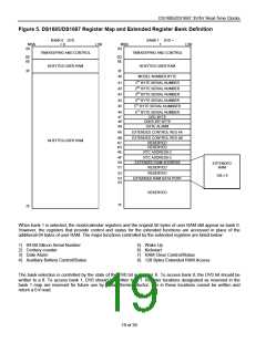
Figure 5. DS1685/DS1687 Register Map and Extended Register Bank Definition
BANK 0 DV0
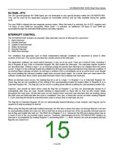
= 0
BANK 1 DV0 =
MSB
00
LSB
MSB
00
1
LSB
TIMEKEEPING AND CONTROL
TIMEKEEPING AND CONTROL
50 BYTES-USER RAM
0D
0E
0D
0E
50 BYTES-USER RAM
3F
3F
40
MODEL NUMBER BYTE
1ST BYTE SERIAL NUMBER
2ND BYTE SERIAL NUMBER
3RD BYTE SERIAL NUMBER
4TH BYTE SERIAL NUMBER
5TH BYTE SERIAL NUMBBER
41
42
43
44
45
46
47
48
49
6TH BYTE SERIAL NUMBER
CRC BYTE
CENTURY BYTE
DATE ALARM
4A
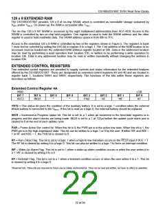
EXTENDED CONTROL REG 4A
4B
4C
4D
EXTENDED CONTROL REG 4B
RESERVED
64 BYTES-USER RAM
RESERVED
4E
RTC ADDRESS-2
4F
50
51
RTC ADDRESS-3
EXTENDED RAM ADDRESS
RESERVED
EXTENDED
RAM
52
53
54
RESERVED
EXTENDED RAM DATA PORT
128 x 8
RESERVED
7F
7F
When bank 1 is selected, the clock/calendar registers and the original 50 bytes of user RAM still appear as bank 0.
However, the registers that provide control and status for the extended functions are accessed in place of the
additional 64 bytes of user RAM. The major functions controlled by the extended registers are listed below:
1) 64-Bit Silicon Serial Number
2) Century counter
5) Wake Up
6) Kickstart
3) Date Alarm
7) RAM Clear Control/Status
8) 128 Bytes Extended RAM Access
4) Auxiliary Battery Control/Status
The bank selection is controlled by the state of the DV0 bit in register A. To access bank 0, the DV0 bit should be
written to a 0. To access bank 1, DV0 should be written to a 1. Register locations designated as reserved in the
bank 1 map are reserved for future use by Dallas Semiconductor. Bits in these locations cannot be written and
return a 0 if read.
19 of 39

 DALLAS [ DALLAS SEMICONDUCTOR ]