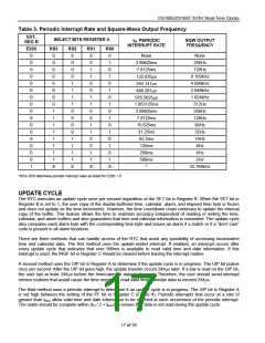
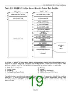
DS1685/DS1687 3V/5V Real-Time Clocks
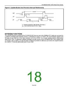
The timing associated with both the wake-up and kickstarting sequences is illustrated in the “Wake-Up/Kickstart
Timing Diagram” in the Electrical Specifications section of this data sheet. The timing associated with these
functions is divided into five intervals, labeled 1 to 5 on the diagram.
The occurrence of either a kickstart or wake-up condition causes the PWR pin to be driven low, as described
above. During Interval 1, if the supply voltage on the DS1685/DS1687 VCC pin rises above the greater of VBAT or
VPF before the power on timeout period (tPOTO) expires, then PWR remains at the active-low level. If VCC does not
rise above the greater of VBAT or VPF in this time, then the PWR output pin is turned off and returns to its high-
impedance level. In this event, the IRQ pin also remains tri-stated. The interrupt flag bit (either WF or KF)
associated with the attempted power-on sequence remains set until cleared by software during a subsequent
system power-on.
If VCC is applied within the timeout period, then the system power-on sequence continues as shown in Intervals 2 to
5 in the timing diagram. During Interval 2, PWR remains active and IRQ is driven to its active-low level, indicating
that either WF or KF was set in initiating the power-on. In the diagram, KS is assumed to be pulled up to the VBAUX
supply. Also at this time, the PAB bit is automatically cleared to 0 in response to a successful power-on. The PWR
line remains active as long as the PAB remains cleared to 0.
At the beginning of Interval 3, the system processor has begun code execution and clears the interrupt condition of
WF and/or KF by writing 0’s to both of these control bits. As long as no other interrupt within the DS1685/DS1687 is
pending, the IRQ line is taken inactive once these bits are reset. Execution of the application software can proceed.
During this time, both the wake-up and kickstart functions can be used to generate status and interrupts. WF is set
in response to a date, hours, minutes, and seconds match condition. KF is set in response to a low-going transition
on KS. If the associated interrupt-enable bit is set (WIE and/or KSE), then the IRQ line is driven active-low in
response to enabled event. In addition, the other possible interrupt sources within the DS1685/DS1687 can cause
IRQ to be driven low. While system power is applied, the on-chip logic always attempts to drive the PWR pin active
in response to the enabled kickstart or wake-up condition. This is true even if PWR was previously inactive as the
result of power being applied by some means other than wake-up or kickstart.
The system can be powered down under software control by setting the PAB bit to a logic 1. This causes the open-
drain PWR pin to be placed in a high-impedance state, as shown at the beginning of Interval 4 in the timing
diagram. As VCC voltage decays, the IRQ output pin is placed in a high-impedance state when VCC goes below VPF.
If the system is to be again powered on in response to a wake-up or kickstart, then the both the WF and KF flags
should be cleared and WIE and/or KSE should be enabled prior to setting the PAB bit.
During Interval 5, the system is fully powered down. Battery backup of the clock calendar and NV RAM is in effect
and IRQ is tri-stated, and monitoring of wake-up and kickstart takes place. If PRS = 1, PWR stays active; otherwise,
if PRS = 0, PWR is tri-stated.
RAM CLEAR
The DS1685/DS1687 provides a RAM clear function for the 242 bytes of user RAM. When enabled, this function
can be performed regardless of the condition of the VCC pin.
The RAM clear function is enabled or disabled by the RAM clear-enable bit (RCE; bank 1, register 04BH). When
RCE is set to a logic 1 and RF=0, the 242 bytes of user RAM is cleared (all bits set to 1) when an active-low
transition is sensed on the RCLR pin. This action has no affect on either the clock/calendar settings or upon the
contents of the extended RAM. The RAM clear flag (RF, bank 1, register 04AH) is set when the RAM clear
operation has been completed. If VCC is present at the time of the RAM clear and RIE = 1, the IRQ line is also
driven low upon completion. The interrupt condition can be cleared by writing a 0 to the RF bit. The IRQ line then
returns to its inactive high level, provided there is no other pending interrupts. Once the RCLR pin is activated, all
read/write accesses are locked out for a minimum recover time, specified as tREC in the Electrical Characteristics
section.
When RCE is cleared to 0, the RAM clear function is disabled. The state of the RCLR pin has no affect on the
contents of the user RAM, and transitions on the RCLR pin have no affect on RF.
21 of 39

 DALLAS [ DALLAS SEMICONDUCTOR ]