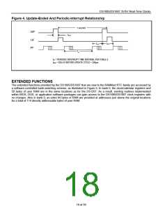
DS1685/DS1687 3V/5V Real-Time Clocks
128 x 8 EXTENDED RAM
The DS1685/DS1687 provides 128 x 8 of on-chip SRAM, which is controlled as nonvolatile storage sustained by
VBAT and/or VBAUX. On power-up, the RAM is accessible after TREC
.
The on-chip 128 x 8 NV SRAM is accessed by the eight multiplexed address/data lines AD7–AD0. Access to the
SRAM is controlled by two on-chip latch registers. One register is used to hold the SRAM address and the other
register is used to hold read/write data. The SRAM address space is from 00h to 7Fh.
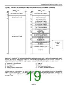
Access to the extended 128 x 8 RAM is controlled by two of the registers shown in Figure 5. The registers in bank
1 must first be selected by setting the DV0 bit in register A to a logic 1. The 7-bit address of the RAM location to be
accessed must be loaded into the extended RAM address register located at 50h. Data in the addressed location
may be read by performing a read operation from location 53h, or written to by performing a write operation to
location 53h. Data in any addressed location may be read or written repeatedly without changing the address in
location 50h.
EXTENDED CONTROL REGISTERS
Two extended control registers are provided to supply controls and status information for the extended features
offered by the DS1685/DS1687. These are designated as extended control registers 4A and 4B and are located in
register bank 1, locations 04AH and 04BH, respectively. The functions of the bits within these registers are
described as follows.
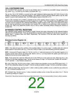
Extended Control Register 4A
MSB
BIT 7
VRT2
LSB
BIT 0
KF
BIT 6
BIT 5
BIT 4
BIT 3
PAB
BIT 2
RF
BIT 1
WF
INCR
*
*
VRT2 – This status bit gives the condition of the auxiliary battery. It is set to a logic 1 condition when the external
lithium battery is connected to the VBAUX. If this bit is read as a logic 0, the external battery should be replaced.
INCR – Increment-in-Progress status bit. This bit is set to a 1 when an increment to the time/date registers is in
progress and the alarm checks are being made. INCR is set to a 1 at 122µs before the update cycle starts and is
cleared to 0 at the end of each update cycle.
PAB – Power-Active Bar control bit. When this bit is 0, the PWR pin is in the active-low state. When this bit is 1, the
PWR pin is in the high-impedance state. This bit can be written to a logic 1 or 0 by the user. If either WF and WIE =
1 or KF and KSE = 1, the PAB bit is cleared to 0.
RF – Ram Clear Flag. This bit is set to a logic 1 when a high-to-low transition occurs on the RCLR input if RCE = 1.
The RF bit is cleared by writing it to a logic 0. This bit can also be written to a logic 1 to force an interrupt condition.
WF – Wake-Up Alarm Flag. This bit is set to 1 when a wake-up alarm condition occurs or when the user writes it to
a 1. WF is cleared by writing it to a 0.
KF – Kickstart Flag. This bit is set to a 1 when a kickstart condition occurs or when the user writes it to a 1. This bit
is cleared by writing it to a logic 0.
*Reserved bits. These bits are reserved for future use by Dallas Semiconductor. They can be read and written, but have no affect on operation.
22 of 39

 DALLAS [ DALLAS SEMICONDUCTOR ]