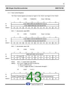
47
8Bit Single Chip Microcontroller
DMC73C168
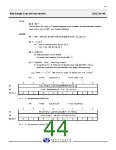
bit of Timer2 has no effect. For right cascading operation, Timer2 is requested to be started first
and then Timer1.
A Timer output function exists on both Timer1 and Timer2 that allows the B0 and B1 outputs,
respectively, to be toggled every timer decrementing through zero.
This function is enabled by the T1OUT bit and T2OUT bit (bit6) in the timer control register
T1CTL0 and T2CTL0.
When operating in the timer output mode, the B0 and/or B1 output can not be changed timer's
START bit will reload and start the timer, but will not toggle the output. The output will toggle
only when the timer decreses through "0". The timer output feature is independent of INT2 and
INT6 and, therefore, will operate with INT2 and INT6 enabled or disabled.
Also, if the timer is active during the IDLE instruction, the timer output feature will continue to
operate. Whenever the T1OUT bit is returned to "0".
B0 or B1 will become an output-only pin like G0. The value in the B0 or B1 data register will be
the last value output by the timer output function. So that B0 or B1 data register will be the last
value output by the timer output function, so that B0 or B1 will not change as the T1OUT or
T2OUT BIT is returned to "0".
Whenever a read of B port is perfomed, the value on the B1 pin will always be returned, so the
current timer output value can be read by reading the B port.
The T1OUT and T2OUT bits are set to 0 by a reset, so the timer output function will not be
enabled unless the user sets T1OUT or T2OUT to 1.
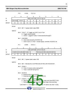
5.5.7 Notes for Timer Usage
In the Timer1 and Timer2, most significant byte readout latch is shared between the most
significant byte (MSB) of the decrement and the MSB of capture latch to be sampled at on
moment. Timer 1 MSB readout latch can be read from both P4 and P6. Similarly, Timer2 MSB
readout latch can be read from both P8 and P10. Reading the LSB of the decrement or capture
latch will always update the content of the readout latch. In order to correctly read the entire
16 bit value of the decrementer or capture latch, the LSB must be read first, which will load the
MSB readout latch. The MSB readout latch must be read and stored after reading the LSB of
either the decrementer or capture latch.
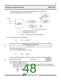
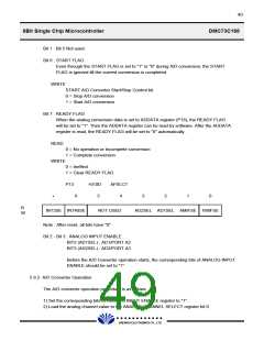
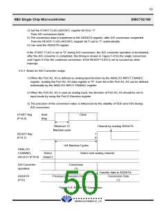
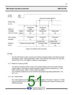
5.6 A/D Converter
The key features of A/D converter are as follows.
- Total Unadjustabled Error
- Analog input
±1 LSB Max
2 channels
- Analog input range
- Conversion
VSS to VDD
Ratiometric Conversion
8 bit
- Resolution
- Conversion time
144 CPU machine cycles
(1 machine cycle = 2/fosc)
£Ä£Á£Å£×£Ï £Ï
DAEWOO ELECTRONICS CO., LTD.

 DAEWOO [ DAEWOO Electronic Components ]