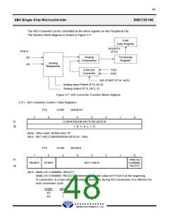
46
8Bit Single Chip Microcontroller
DMC73C168
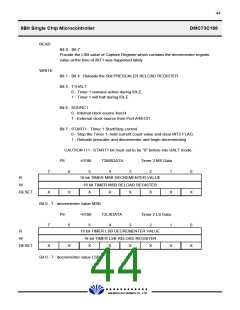
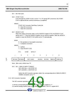
5.5.2 Real Time Clock mode (RTC)
In the Real Time Clock mode, Fosc/4 which is internally generated is the decrementer clock source.
Each positive pulse transition of the Fosc/4 period signal decrements the count chain.
5.5.3 Event Counter mode (EC)
When Timer1 or Timer2 is selected to use in the EC mode, pin A4 and A5 operate as clock source
decrementers for Timer1 and Timer2, respectively. The maximum clock frequency on A4 and A5
in the EC mode must not be greater than fosc/4. The minimum pulse width must not be less than
1.24 state clock cycles. Each positive pulse transition decreases the count chain.
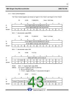
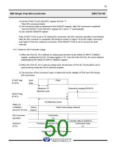
5.5.4 Timer and Prescaled Clock
The timer clock, whether internal or external, is prescaled by a 5-bit module-N counter. The actual
prescaling value is determined by the least significant five bits of the timer control register, and the
actual prescaling value is equal to the timer control latch value plus one.
An INT2 interrupt for Timer1 and INT6 interrupt for Timer2 are momentarily pulsed when both the
prescaler and counter is decreased to zero value together. This sets the INT2 or INT6 flag flip-flop.
The prescaler and counter and then immediately reloaded with the contents of the prescale latch
(PL) and the timer latch (TL) and the timer will start decreasing with the PL and TL value.
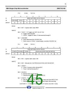
5.5.5 Timer Interrupt Pulses
The period of the timer INT2 and INT6 interrupt pulses may be calculated by following formula :
tINT = tCLK * (PL + 1) * (TL + 1)
where
tINT = period of timer interrupt
tCLK = 4/Fosc for internal Real Time Clock mode or the
period of input external EC mode
PL = Prescaler Latch value
TL = Timer Latch value
At the falling edge of the INT3 and INT1 input, the Timer1 and Timer2 values are loaded into the
corresponding Capture Latch (CL), when read Timer1 and Timer2 control register contain the CL
value. This feature provides the capability to determine when an external event occurred relative
to the internal timer.
5.5.6 Timer Output Function
Timer1 and Timer2 can be cascaded together to form one large timer by setting the CASCADE
bit of T2CTL0 (P10) to "1". The CASCADE bit of 1 selects the output generated by Timer1 reload
pulse as the clock input to the prescaler of Timer 2.
The CASCADE bit overrides the SOURCE bit, that is, if the CASCADE bit is "1", the SOURCE
£Ä£Á£Å£×£Ï £Ï
DAEWOO ELECTRONICS CO., LTD.

 DAEWOO [ DAEWOO Electronic Components ]