41
8Bit Single Chip Microcontroller
DMC73C168
5.5 Programmable Timer / Event Counter
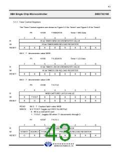
DMC73C168 features two on-chip timers with individual start and stop bits. Timer1 and Timer2 (shown
in Fig. 5-5 & Fig 5-6) consist of a 16 bit capture latch, and a 5-bit non-readable prescaler with a 5-bit
reload register.
The clock source of Timer1 and Timer2 shown in Table 5-1 is determined by bit 6 (SOURCE) of T1CLT1
and T2CTL1 respectively. A SOURCE bit of 0 selects the internally generated Fosc/4 clock and places
the Timer/Event Counter in the Real Timer Clock (RTC) mode. A SOURCE bit of 1 selects the external
clock source and places the Timer/Event Counter in the Event counter mode. In the external mode,
the clock source for Timer 1 and 2 are input on the two least significant Bits of I/O Port A(A4) and (A5)
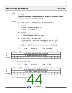
respectively. Bit 7 of the timer control registers is the START bit for the respective programmable timers.
When a 0 is written to the START bit, regardless of whether it was a 0 or 1 before, the prescaler and
counter decrementers are loaded with the corresponding latch values, and the Timer/Event Counter
operation begins. When the prescaler and counter decrement through zero together, an interrupt flag is
set and the prescaler and counter decrementers are immediately and automatically reloaded with the
corresponding latch values.
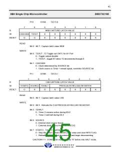
The interrupt levels generated by the timers are INT2 for Timer1 and INT6 for Timer2. Timer1 and Timer2
each have a 16-bit Capture Latch (CL) associated with them which capture the current value of the
counter whenever INT3 for Timer1 and INT1 for Timer2 are triggered. The capture latch will store the
Timer value even when INT1/INT3 are disabled. Both capture latch is disabled during the IDLE instruction
when their corresponding timer HALT bits are 1.
Table 5-1. Timer 1 & Timer 2 clock Sources
Timer
1
Mode
Source Cascade Clock Source
Capture Latch Interrupt
Trigger
Bit
Bit
RTC
EC
0
-
Fosc/4
External Port A4
Fosc/4
INT3
INT2
1
-
RTC
0
-
2
EC
1
-
External Port A5
Timer1
INT1
INT6
CASCADE
-
1
In the Timer1 and Timer2, most significant byte readout latch is shared between the most significant
byte (MSB) of the decrementer and the MSB of the capture latch. It allows the complete 16-bit value of
the decrementer or the capture latch to be sampled at one moment. The least significant byte (LSB)
must be read first, which causes the MSB to be simultaneously loaded into the readout latch.
There is only one readout latch for each timer, but the some latch can be read from two address for
easier programming (see the diagrams for Timer1 and Timer2)
Timer1 MSB readout latch can be read from both P4(>0104) P6(>0106).
Similarly, Timer2 MSB readout latch can be read from both P8(>0108) and P10(010A)
Reading the LSB of the decrementer or capture latch will always update the contents of the readout
latch. In order to correctly read the entire 16-bit value of the decrementer or capture, the LSB must be
read first, which will load the MSB readout latch. The MSB readout latch must be read and stored
before reading the LSB of either the decrementer or capture latch.
£Ä£Á£Å£×£Ï £Ï
DAEWOO ELECTRONICS CO., LTD.

 DAEWOO [ DAEWOO Electronic Components ]