PSoC® 3: CY8C32 Family
Data Sheet
11.1 Inputs and Outputs
Specifications are valid for –40 °C ≤ TA ≤ 85 °C and TJ ≤ 100 °C, except where noted. Specifications are valid for 1.71 V to 5.5 V,
except where noted. Unless otherwise specified, all charts and graphs show typical values.
11.1.1 GPIO
Table 11-9. GPIO DC Specifications
Parameter
Description
Input voltage high threshold
Input voltage low threshold
Input voltage high threshold
Conditions
CMOS Input, PRT[×]CTL = 0 0.7 × VDDIO
CMOS Input, PRT[×]CTL = 0
Min
Typ
–
Max
Units
VIH
VIL
VIH
–
V
V
V
–
–
0.3 × VDDIO
LVTTL Input, PRT[×]CTL = 0.7 × VDDIO
1, VDDIO < 2.7 V
–
–
VIH
VIL
Input voltage high threshold
Input voltage low threshold
Input voltage low threshold
Output voltage high
LVTTL Input, PRT[×]CTL =
1, VDDIO ≥ 2.7V
2.0
–
–
–
–
0.3 × VDDIO
0.8
V
V
V
LVTTL Input, PRT[×]CTL =
1, VDDIO < 2.7 V
–
VIL
LVTTL Input, PRT[×]CTL =
1, VDDIO ≥ 2.7V
–
VOH
IOH = 4 mA at 3.3 VDDIO
IOH = 1 mA at 1.8 VDDIO
IOL = 8 mA at 3.3 VDDIO
IOL = 4 mA at 1.8 VDDIO
VDDIO – 0.6
–
–
–
–
V
V
VDDIO – 0.5
VOL
Output voltage low
Pull-up resistor
–
–
–
0.6
0.6
8.5
8.5
2
V
–
V
Rpullup
3.5
3.5
–
5.6
5.6
–
kΩ
kΩ
nA
pF
mV
µA
Rpulldown Pull-down resistor
IIL
Input leakage current (absolute value)[29]
Input capacitance[29]
Input voltage hysteresis (Schmitt-Trigger)[29]
25 °C, VDDIO = 3.0 V
CIN
VH
–
–
7
–
40
–
–
Idiode
Current through protection diode to VDDIO and
VSSIO
–
100
Rglobal
Rmux
Resistance pin to analog global bus
Resistance pin to analog mux bus
25 °C, VDDIO = 3.0 V
25 °C, VDDIO = 3.0 V
–
–
320
220
–
–
Ω
Ω
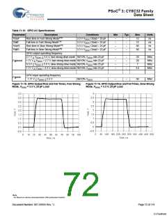
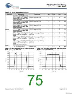
Figure 11-13. GPIO Output High Voltage and Current
Figure 11-14. GPIO Output Low Voltage and Current
Note
28. Based on device characterization (Not production tested).
Document Number: 001-56955 Rev. *J
Page 71 of 119
[+] Feedback

 CYPRESS [ CYPRESS ]