PSoC® 3: CY8C32 Family
Data Sheet
Table 11-3. AC Specifications[22]
Parameter Description
FCPU
Conditions
1.71 V ≤ VDDD ≤ 5.5 V
1.71 V ≤ VDDD ≤ 5.5 V
Min
DC
DC
–
Typ
–
Max
50.01
50.01
1
Units
MHz
MHz
V/ns
µs
CPU frequency
Bus frequency
FBUSCLK
Svdd
–
VDD ramp rate
–
TIO_INIT
Time from VDDD/VDDA/VCCD/VCCA
≥ IPOR to I/O ports set to their reset
states
–
–
10
TSTARTUP
Time from VDDD/VDDA/VCCD/VCCA
≥ PRES to CPU executing code at VDDA/VDDD, no PLL used, IMO
reset vector
V
CCA/VCCD = regulated from
–
–
–
–
66
15
µs
µs
boot mode (12 MHz typ.)
TSLEEP
Wakeup from sleep mode –
Application of non-LVD interrupt to
beginning of execution of next CPU
instruction
THIBERNATE
Wakeup from hibernate mode –
Application of external interrupt to
beginning of execution of next CPU
instruction
–
–
100
µs
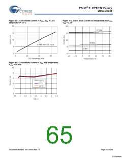
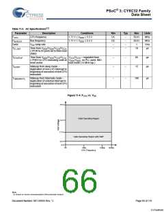
Figure 11-4. FCPU vs. VDD
5.5 V
Valid Operating Region
3.3 V
1.71 V
0.5 V
Valid Operating Region with SMP
0 V
DC
1 MHz
10 MHz
50 MHz
CPU Frequency
Note
22. Based on device characterization (Not production tested).
Document Number: 001-56955 Rev. *J
Page 66 of 119
[+] Feedback

 CYPRESS [ CYPRESS ]