PSoC® 3: CY8C32 Family
Data Sheet
11. Electrical Specifications
Specifications are valid for –40 °C ≤ TA ≤ 85 °C and TJ ≤ 100 °C, except where noted. Specifications are valid for 1.71 V to 5.5 V,
except where noted. The unique flexibility of the PSoC UDBs and analog blocks enable many functions to be implemented in PSoC
Creator components, see the component datasheets for full AC/DC specifications of individual functions. See the “Example
Peripherals” section on page 41 for further explanation of PSoC Creator components.
11.1 Absolute Maximum Ratings
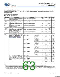
Table 11-1. Absolute Maximum Ratings DC Specifications
Parameter
TSTG
Description
Storage temperature
Conditions
Min
Typ
Max
Units
Higher storage temperatures
reduce NVL data retention time.
Recommended storage temper-
ature is +25 °C ±25 °C. Extended
duration storage temperatures
above 85 °C degrade reliability.
–55
25
100
°C
VDDA
VDDD
Analog supply voltage relative to
VSSA
–0.5
–0.5
–
–
6
6
V
V
Digital supply voltage relative to
VSSD
VDDIO
VCCA
VCCD
VSSA
I/O supply voltage relative to VSSD
Direct analog core voltage input
Direct digital core voltage input
Analog ground voltage
–0.5
–0.5
–
–
–
–
6
V
V
V
V
1.95
1.95
–0.5
VSSD –0.5
VSSD
0.5
+
[14]
VGPIO
DC input voltage on GPIO
DC input voltage on SIO
Includes signals sourced by VDDA VSSD –0.5
and routed internal to the pin
–
VDDIO
0.5
+
V
VSIO
Output disabled
Output enabled
VSSD –0.5
–
–
–
–
–
–
–
–
–
7
6
V
V
VSSD –0.5
VIND
Voltage at boost converter input
Boost converter supply
0.5
VSSD –0.5
–
5.5
5.5
100
2
V
VBAT
Ivddio
V
Current per VDDIO supply pin
ADC external reference inputs
Latch up current[15]
mA
V
Vextref
LU
Pins P0[3], P3[2]
–
–140
750
140
–
mA
V
ESDHBM
ESDCDM
Electrostatic discharge voltage
Electrostatic discharge voltage
Human body model
Charge device model
500
–
V
Note Usage above the absolute maximum conditions listed in Table 11-1 may cause permanent damage to the device. Exposure to
maximum conditions for extended periods of time may affect device reliability. When used below maximum conditions but above
normal operating conditions the device may not operate to specification.
Notes
14. The VDDIO supply voltage must be greater than the maximum analog voltage on the associated GPIO pins. Maximum analog voltage on GPIO pin ≤ VDDIO ≤ VDDA
15. Meets or exceeds JEDEC Spec EIA/JESD78 IC Latch-up Test.
.
Document Number: 001-56955 Rev. *J
Page 62 of 119
[+] Feedback

 CYPRESS [ CYPRESS ]