CY8C24x23 Final Data Sheet
3. Electrical Specifications
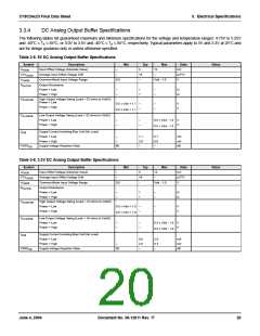
3.3.8
DC POR and LVD Specifications
The following table lists guaranteed maximum and minimum specifications for the voltage and temperature ranges: 4.75V to 5.25V
and -40°C ≤ T ≤ 85°C, or 3.0V to 3.6V and -40°C ≤ T ≤ 85°C, respectively. Typical parameters apply to 5V and 3.3V at 25°C and
A
A
are for design guidance only or unless otherwise specified.
Note The bits PORLEV and VM in the table below refer to bits in the VLT_CR register. See the PSoC Mixed Signal Array Technical
Reference Manual for more information on the VLT_CR register.
Table 3-14. DC POR and LVD Specifications
Symbol
Description
Min
Typ
Max
Units
Notes
Vdd Value for PPOR Trip (positive ramp)
PORLEV[1:0] = 00b
V
V
V
PPOR0R
PPOR1R
PPOR2R
2.908
V
V
V
PORLEV[1:0] = 01b
–
–
4.394
4.548
–
–
PORLEV[1:0] = 10b
Vdd Value for PPOR Trip (negative ramp)
PORLEV[1:0] = 00b
V
V
V
PPOR0
PPOR1
PPOR2
2.816
4.394
4.548
V
V
V
PORLEV[1:0] = 01b
PORLEV[1:0] = 10b
PPOR Hysteresis
V
V
V
PH0
PH1
PH2
PORLEV[1:0] = 00b
PORLEV[1:0] = 01b
PORLEV[1:0] = 10b
–
–
–
92
0
–
–
–
mV
mV
mV
0
Vdd Value for LVD Trip
VM[2:0] = 000b
VM[2:0] = 001b
VM[2:0] = 010b
VM[2:0] = 011b
VM[2:0] = 100b
VM[2:0] = 101b
VM[2:0] = 110b
VM[2:0] = 111b
V
V
V
V
V
V
V
V
a
LVD0
LVD1
LVD2
LVD3
LVD4
LVD5
LVD6
LVD7
V
2.863
2.963
3.070
3.920
4.393
4.550
4.632
4.718
2.921
3.023
3.133
4.00
2.979
3.083
3.196
4.080
4.573
V
V
V
V
V
V
V
V
4.483
4.643
4.727
4.814
b
4.736
4.822
4.910
Vdd Value for PUMP Trip
VM[2:0] = 000b
VM[2:0] = 001b
VM[2:0] = 010b
VM[2:0] = 011b
VM[2:0] = 100b
VM[2:0] = 101b
VM[2:0] = 110b
VM[2:0] = 111b
V
V
V
V
V
V
V
V
V
V
V
V
V
V
V
V
V
2.963
3.033
3.185
4.110
4.550
4.632
4.719
4.900
3.023
3.095
3.250
4.194
4.643
4.727
4.815
5.000
3.083
3.157
3.315
4.278
4.736
4.822
4.911
5.100
PUMP0
PUMP1
PUMP2
PUMP3
PUMP4
PUMP5
PUMP6
PUMP7
a. Always greater than 50 mV above PPOR (PORLEV = 00) for falling supply.
b. Always greater than 50 mV above PPOR (PORLEV = 10) for falling supply.
June 4, 2004
Document No. 38-12011 Rev. *F
24

 CYPRESS [ CYPRESS ]