CY8C24x23 Final Data Sheet
3. Electrical Specifications
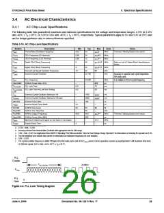
3.4
AC Electrical Characteristics
3.4.1
AC Chip-Level Specifications
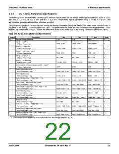
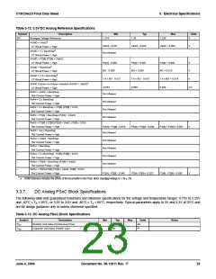
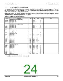
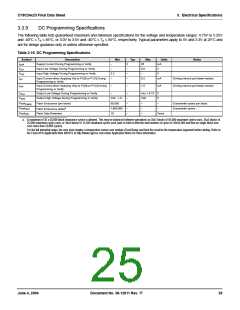
The following table lists guaranteed maximum and minimum specifications for the voltage and temperature ranges: 4.75V to 5.25V
and -40°C ≤ T ≤ 85°C, or 3.0V to 3.6V and -40°C ≤ T ≤ 85°C, respectively. Typical parameters apply to 5V and 3.3V at 25°C and
A
A
are for design guidance only or unless otherwise specified.
Table 3-16. AC Chip-Level Specifications
Symbol
IMO
Description
Min
23.4
Typ
Max
Units
MHz
Notes
a
F
F
F
F
Internal Main Oscillator Frequency
24
24
12
48
Trimmed. Utilizing factory trim values.
24.6
a,b
CPU Frequency (5V Nominal)
CPU Frequency (3.3V Nominal)
Digital PSoC Block Frequency
0.93
0.93
0
MHz
MHz
MHz
CPU1
CPU2
48M
24.6
12.3
49.2
b,c
a,b,d
Refer to the AC Digital Block Specifications
below.
b,e,d
F
F
F
Digital PSoC Block Frequency
Internal Low Speed Oscillator Frequency
External Crystal Oscillator
0
24
32
MHz
kHz
kHz
24M
24.6
64
15
–
32K1
32K2
32.768
–
Accuracy is capacitor and crystal dependent.
50% duty cycle.
F
PLL Frequency
–
23.986
–
MHz
Is a multiple (x732) of crystal frequency.
PLL
Jitter24M2
24 MHz Period Jitter (PLL)
PLL Lock Time
–
–
–
600
10
ps
T
0.5
ms
PLLSLEW
T
PLL Lock Time for Low Gain Setting
0.5
–
50
ms
PLLSLEWS-
LOW
T
External Crystal Oscillator Startup to 1%
–
–
1700
2800
ms
ms
OS
2620
3800
f
T
External Crystal Oscillator Startup to 100 ppm
OSACC
Jitter32k
32 kHz Period Jitter
–
100
–
ns
T
External Reset Pulse Width
10
–
µs
XRST
DC24M
24 MHz Duty Cycle
40
–
50
60
–
%
Step24M
Fout48M
24 MHz Trim Step Size
48 MHz Output Frequency
50
kHz
MHz
a,c
46.8
48.0
Trimmed. Utilizing factory trim values.
49.2
Jitter24M1
24 MHz Period Jitter (IMO)
–
–
600
–
ps
F
T
Maximum frequency of signal on row input or row output.
12.3
–
MHz
MAX
Supply Ramp Time
0
–
µs
RAMP
a. 4.75V < Vdd < 5.25V.
b. Accuracy derived from Internal Main Oscillator with appropriate trim for Vdd range.
c. 3.0V < Vdd < 3.6V. See Application Note AN2012 “Adjusting PSoC Microcontroller Trims for Dual Voltage-Range Operation” for information on trimming for operation at 3.3V.
d. See the individual user module data sheets for information on maximum frequencies for user modules.
e. 3.0V < 5.25V.
f. The crystal oscillator frequency is within 100 ppm of its final value by the end of the T
period. Correct operation assumes a properly loaded 1 uW maximum drive level
osacc
o
o
32.768 kHz crystal. 3.0V ≤ Vdd ≤ 5.5V, -40 C ≤ T ≤ 85 C.
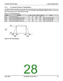
A
PLL
Enable
T
24 MHz
PLLSLEW
FPLL
PLL
Gain
0
Figure 3-3. PLL Lock Timing Diagram
June 4, 2004
Document No. 38-12011 Rev. *F
26

 CYPRESS [ CYPRESS ]