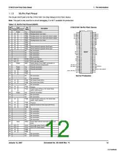
1. Pin Information
This chapter describes, lists, and illustrates the CY8C21x34 PSoC device pins and pinout configurations.
1.1
Pinouts
The CY8C21x34 PSoC device is available in a variety of packages which are listed and illustrated in the following tables. Every port
pin (labeled with a “P”) is capable of Digital IO and connection to the common analog bus. However, Vss, Vdd, SMP, and XRES are
not capable of Digital IO.
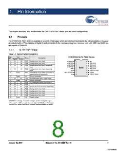
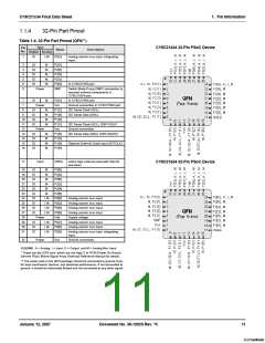
1.1.1
16-Pin Part Pinout
Table 1-1. 16-Pin Part Pinout (SOIC)
Type
Pin
CY8C21234 16-Pin PSoC Device
Name
Description
No.
Digital Analog
1
2
3
IO
IO
IO
I, M
I, M
I, M
P0[7] Analog column mux input.
P0[5] Analog column mux input.
A, I,M, P0[7]
A, I,M, P0[5]
A, I,M, P0[3]
A, I,M, P0[1]
SMP
Vdd
1
2
3
4
5
6
7
8
16
15
14
13
12
11
10
9
P0[6], A,I, M
P0[4], A,I, M
P0[2], A,I, M
P0[0], A,I, M
P1[4],EXTCLK,M
P1[2],M
P0[3] Analog column mux input, integrating
input.
SOIC
4
5
IO
I, M
P0[1] Analog column mux input, integrating
input.
Vss
M,I2CSCL,P1[1]
Vss
Power
Power
SMP
Switch Mode Pump (SMP) connection to
required external components.
P1[0],I2CSDA,M
6
Vss
Ground connection.
7
IO
M
P1[1] I2C Serial Clock (SCL), ISSP-SCLK*.
Vss Ground connection.
8
Power
9
IO
IO
IO
IO
IO
IO
IO
M
M
P1[0] I2C Serial Data (SDA), ISSP-SDATA*.
P1[2]
10
11
12
13
14
15
16
M
P1[4] Optional External Clock Input (EXTCLK).
P0[0] Analog column mux input.
P0[2] Analog column mux input.
P0[4] Analog column mux input.
P0[6] Analog column mux input.
I, M
I, M
I, M
I, M
Power
Vdd
Supply voltage.
LEGEND A = Analog, I = Input, O = Output, and M = Analog Mux Input.
* These are the ISSP pins, which are not High Z at POR (Power On Reset).
See the PSoC Mixed-Signal Array Technical Reference Manual for details.
January 12, 2007
Document No. 38-12025 Rev. *K
8
[+] Feedback

 CYPRESS [ CYPRESS ]