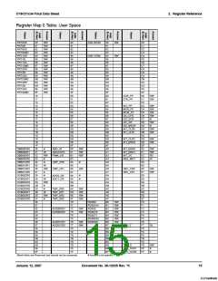
CY8C21x34 Final Data Sheet
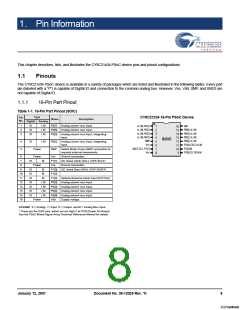
1. Pin Information
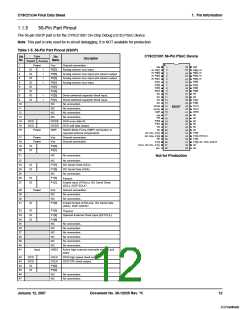
1.1.5
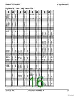
56-Pin Part Pinout
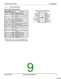
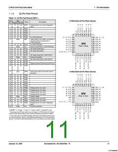
The 56-pin SSOP part is for the CY8C21001 On-Chip Debug (OCD) PSoC device.
Note This part is only used for in-circuit debugging. It is NOT available for production.
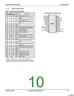
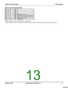
Table 1-5. 56-Pin Part Pinout (SSOP)
Type
CY8C21001 56-Pin PSoC Device
Pin
No.
Pin
Name
Description
Digital Analog
1
Power
Vss
Ground connection.
Vss
56
55
Vdd
1
2
2
IO
IO
IO
IO
IO
IO
IO
IO
I
I
I
I
P0[7]
P0[5]
P0[3]
P0[1]
P2[7]
P2[5]
P2[3]
P2[1]
NC
Analog column mux input.
AI, P0[7]
AI, P0[5]
AI, P0[3]
P0[6], AI
P0[4], AI
P0[2], AI
3
4
5
6
54
53
3
Analog column mux input and column output.
Analog column mux input and column output.
Analog column mux input.
4
AI, P0[1]
P2[7]
P2[5]
P2[3]
P2[1]
NC
P0[0], AI
P2[6]
52
51
5
P2[4]
P2[2]
P2[0]
NC
7
8
9
50
49
48
6
7
10
47
46
45
44
43
42
41
40
39
38
37
36
35
34
8
I
I
Direct switched capacitor block input.
Direct switched capacitor block input.
No connection.
NC
NC
NC
NC
11
12
13
9
P3[2]
P3[0]
CCLK
HCLK
XRES
NC
10
11
12
13
14
15
16
OCDE
OCDO
SMP
14
SSOP
NC
No connection..
15
16
NC
No connection.
17
Vss
Vss
NC
No connection..
NC
NC
NC
18
19
20
P3[3]
P3[1]
NC
OCD
OCD
OCDE
OCD even data IO.
OCDO OCD odd data output.
NC
21
22
23
NC
Power
SMP
Switch Mode Pump (SMP) connection to
required external components.
NC
P1[6]
I2C SCL, P1[7]
P1[4], EXTCLK
P1[2]
I2C SDA, P1[5]
NC
24
25
33
32
17
18
19
20
Power
Power
Vss
Ground connection.
Vss
Ground connection.
P1[3]
SCLK, I2C SCL, P1[1]
Vss
P1[0], I2C
NC
SDA, SDATA
26
27
28
31
30
IO
IO
P3[3]
P3[1]
NC
29
21
NC
No connection.
Not for Production
22
23
24
25
26
NC
No connection..
IO
IO
P1[7]
P1[5]
NC
I2C Serial Clock (SCL).
I2C Serial Data (SDA).
No connection.
IO
IO
P1[3]
I
.
FMTEST
27
P1[1]
Crystal Input (XTALin), I2C Serial Clock
(SCL), ISSP-SCLK*.
28
29
30
31
Power
Vss
NC
Ground connection.
No connection.
NC
No connection..
IO
IO
P1[0]
Crystal Output (XTALout), I2C Serial Data
(SDA), ISSP-SDATA*.
32
P1[2]
V
.
FMTEST
33
34
35
36
37
38
39
40
41
IO
IO
P1[4]
P1[6]
NC
Optional External Clock Input (EXTCLK).
No connection..
No connection.
No connection..
No connection.
No connection..
No connection..
NC
NC
NC
NC
NC
Input
XRES
Active high external reset with internal pull
down.
42
43
44
45
46
47
OCD
OCD
IO
HCLK
CCLK
P3[0]
P3[2]
NC
OCD high-speed clock output.
OCD CPU clock output.
IO
No connection.
No connection..
NC
January 12, 2007
Document No. 38-12025 Rev. *K
12
[+] Feedback

 CYPRESS [ CYPRESS ]