CY8C21x34 Final Data Sheet
1. Pin Information
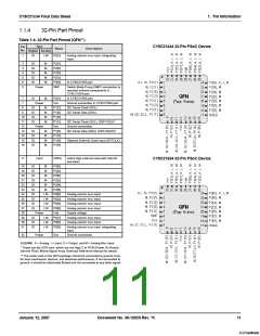
1.1.4
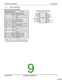
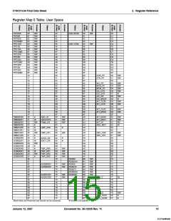
32-Pin Part Pinout
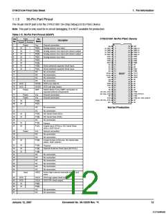
Table 1-4. 32-Pin Part Pinout (QFN**)
Type
Pin
CY8C21434 32-Pin PSoC Device
Name
Description
No.
Digital Analog
1
IO
I, M
P0[1]
Analog column mux input, integrating
input.
2
3
4
5
6
6
IO
IO
IO
IO
IO
M
M
M
M
M
P2[7]
P2[5]
P2[3]
P2[1]
P3[3]
SMP
In CY8C21434 part.
Power
Switch Mode Pump (SMP) connection to
required external components in
CY8C21634 part.
7
IO
M
P3[1]
Vss
In CY8C21434 part.
7
Power
Power
Ground connection in CY8C21634 part.
I2C Serial Clock (SCL).
8
IO
IO
IO
IO
M
M
M
M
P1[7]
P1[5]
P1[3]
P1[1]
Vss
9
I2C Serial Data (SDA).
10
11
12
13
14
15
16
I2C Serial Clock (SCL), ISSP-SCLK*.
Ground connection.
IO
IO
IO
IO
M
M
M
M
P1[0]
P1[2]
P1[4]
P1[6]
I2C Serial Data (SDA), ISSP-SDATA*.
Optional External Clock Input (EXTCLK).
17
Input
XRES
Active high external reset with internal
pull down.
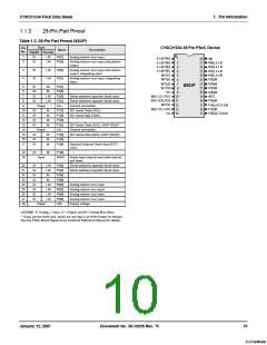
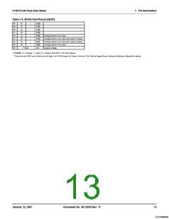
CY8C21634 32-Pin PSoC Device
18
19
20
21
22
23
24
25
26
27
28
29
30
31
IO
IO
IO
IO
IO
IO
IO
IO
IO
IO
M
M
M
M
M
M
P3[0]
P3[2]
P2[0]
P2[2]
P2[4]
P2[6]
P0[0]
P0[2]
P0[4]
P0[6]
Vdd
I, M
I, M
I, M
I, M
Analog column mux input.
Analog column mux input.
Analog column mux input.
Analog column mux input.
Supply voltage.
Power
IO
IO
IO
I, M
I, M
I, M
P0[7]
P0[5]
P0[3]
Analog column mux input.
Analog column mux input.
Analog column mux input, integrating
input.
32
Power
Vss
Ground connection.
LEGEND A = Analog, I = Input, O = Output, and M = Analog Mux Input.
* These are the ISSP pins, which are not High Z at POR (Power On Reset).
See the PSoC Mixed-Signal Array Technical Reference Manual for details.
** The center pad on the QFN package should be connected to ground (Vss)
for best mechanical, thermal, and electrical performance. If not connected to
ground, it should be electrically floated and not connected to any other signal.
January 12, 2007
Document No. 38-12025 Rev. *K
11
[+] Feedback

 CYPRESS [ CYPRESS ]