CY8C21x34 Final Data Sheet
3. Electrical Specifications
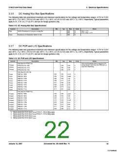
3.3.6
DC Analog Mux Bus Specifications
The following table lists guaranteed maximum and minimum specifications for the voltage and temperature ranges: 4.75V to 5.25V
and -40°C ≤ TA ≤ 85°C, 3.0V to 3.6V and -40°C ≤ TA ≤ 85°C, or 2.4V to 3.0V and -40°C ≤ TA ≤ 85°C, respectively. Typical parameters
apply to 5V, 3.3V, or 2.7V at 25°C and are for design guidance only.
Table 3-12. DC Analog Mux Bus Specifications
Symbol
Description
Min
Typ
Max
400
800
Units
Notes
R
R
Switch Resistance to Common Analog Bus
–
–
–
–
Ω
Ω
Vdd ≥ 2.7V
2.4V ≤ Vdd ≤ 2.7V
SW
Resistance of Initialization Switch to Vdd
800
Ω
VDD
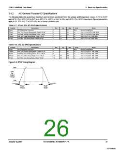
3.3.7
DC POR and LVD Specifications
The following table lists guaranteed maximum and minimum specifications for the voltage and temperature ranges: 4.75V to 5.25V
and -40°C ≤ TA ≤ 85°C, 3.0V to 3.6V and -40°C ≤ TA ≤ 85°C, or 2.4V to 3.0V and -40°C ≤ TA ≤ 85°C, respectively. Typical parameters
apply to 5V, 3.3V, or 2.7V at 25°C and are for design guidance only.
Table 3-13. DC POR and LVD Specifications
Symbol
Description
Vdd Value for PPOR Trip
Min
Typ
Max
Units
Notes
Vdd must be greater than or equal to 2.5V
during startup, reset from the XRES pin, or
reset from Watchdog.
V
V
V
PPOR0
PPOR1
PPOR2
PORLEV[1:0] = 00b
PORLEV[1:0] = 01b
PORLEV[1:0] = 10b
Vdd Value for LVD Trip
VM[2:0] = 000b
2.36
2.40
V
V
V
–
2.82
4.55
2.95
4.70
a
b
V
V
V
V
V
V
V
V
2.40
2.85
2.95
3.06
4.37
4.50
4.62
4.71
2.45
2.92
3.02
3.13
4.48
4.64
4.73
4.81
2.51
2.99
3.09
3.20
4.55
4.75
4.83
4.95
V
V
V
V
V
V
V
V
LVD0
LVD1
LVD2
LVD3
LVD4
LVD5
LVD6
LVD7
VM[2:0] = 001b
VM[2:0] = 010b
VM[2:0] = 011b
VM[2:0] = 100b
VM[2:0] = 101b
VM[2:0] = 110b
VM[2:0] = 111b
Vdd Value for PUMP Trip
VM[2:0] = 000b
VM[2:0] = 001b
VM[2:0] = 010b
VM[2:0] = 011b
VM[2:0] = 100b
VM[2:0] = 101b
VM[2:0] = 110b
VM[2:0] = 111b
c
V
V
V
V
V
V
V
V
2.45
2.96
3.03
3.18
4.54
4.62
4.71
4.89
2.55
3.02
3.10
3.25
4.64
4.73
4.82
5.00
V
V
V
V
V
V
V
V
2.62
3.09
3.16
3.32
4.74
4.83
4.92
5.12
PUMP0
PUMP1
PUMP2
PUMP3
PUMP4
PUMP5
PUMP6
PUMP7
d
a. Always greater than 50 mV above VPPOR (PORLEV = 00) for falling supply.
b. Always greater than 50 mV above VPPOR (PORLEV = 01) for falling supply.
c. Always greater than 50 mV above V
d. Always greater than 50 mV above V
.
.
LVD0
LVD3
January 12, 2007
Document No. 38-12025 Rev. *K
22
[+] Feedback

 CYPRESS [ CYPRESS ]