CY8C21x34 Final Data Sheet
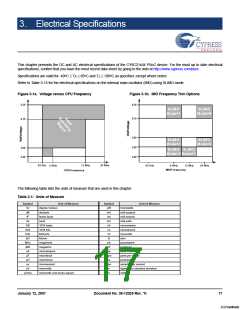
3. Electrical Specifications
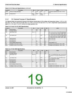
Table 3-4. DC Chip-Level Specifications (continued)
Symbol
Description
Reference Voltage (Bandgap)
Min
1.16
Typ
1.30
Max
1.33
Units
Notes
V
REF27
V
V
Trimmed for appropriate Vdd. Vdd = 2.4V to
3.0V.
AGND
Analog Ground
V
V
V
REF
REF
REF
- 0.003
+ 0.003
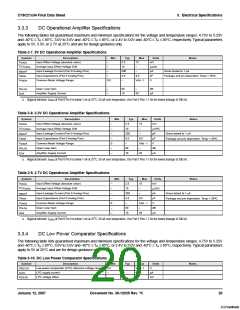
3.3.2
DC General Purpose IO Specifications
The following tables list guaranteed maximum and minimum specifications for the voltage and temperature ranges: 4.75V to 5.25V
and -40°C ≤ TA ≤ 85°C, 3.0V to 3.6V and -40°C ≤ TA ≤ 85°C, or 2.4V to 3.0V and -40°C ≤ TA ≤ 85°C, respectively. Typical parameters
apply to 5V, 3.3V, and 2.7V at 25°C and are for design guidance only.
Table 3-5. 5V and 3.3V DC GPIO Specifications
Symbol
Description
Min
Typ
5.6
Max
Units
kΩ
Notes
R
Pull-up Resistor
4
4
8
8
–
PU
PD
OH
R
Pull-down Resistor
High Output Level
5.6
–
kΩ
V
Vdd - 1.0
V
IOH = 10 mA, Vdd = 4.75 to 5.25V (8 total loads,
4 on even port pins (for example, P0[2], P1[4]),
4 on odd port pins (for example, P0[3], P1[5])).
V
Low Output Level
–
–
0.75
0.8
V
IOL = 25 mA, Vdd = 4.75 to 5.25V (8 total loads,
4 on even port pins (for example, P0[2], P1[4]),
4 on odd port pins (for example, P0[3], P1[5])).
OL
V
V
V
I
Input Low Level
Input High Level
Input Hysteresis
–
–
V
Vdd = 3.0 to 5.25.
Vdd = 3.0 to 5.25.
IL
IH
H
2.1
–
–
V
60
1
–
mV
nA
pF
pF
Input Leakage (Absolute Value)
Capacitive Load on Pins as Input
Capacitive Load on Pins as Output
–
–
Gross tested to 1 µA.
IL
o
C
C
–
3.5
3.5
10
10
Package and pin dependent. Temp = 25 C.
IN
o
–
Package and pin dependent. Temp = 25 C.
OUT
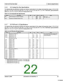
Table 3-6. 2.7V DC GPIO Specifications
Symbol
Description
Min
Typ
Max
Units
Notes
R
Pull-up Resistor
4
5.6
5.6
–
8
8
–
kΩ
kΩ
V
PU
PD
OH
R
Pull-down Resistor
High Output Level
4
V
Vdd - 0.4
IOH = 2.5 mA (6.25 Typ), Vdd = 2.4 to 3.0V (16
mA maximum, 50 mA Typ combined IOH bud-
get).
V
OL
Low Output Level
–
–
0.75
V
IOL = 10 mA, Vdd = 2.4 to 3.0V (90 mA maxi-
mum combined IOL budget).
V
V
V
I
Input Low Level
Input High Level
Input Hysteresis
–
–
0.75
–
V
Vdd = 2.4 to 3.0.
Vdd = 2.4 to 3.0.
IL
IH
H
2.0
–
–
V
90
1
–
mV
nA
pF
pF
Input Leakage (Absolute Value)
Capacitive Load on Pins as Input
Capacitive Load on Pins as Output
–
–
Gross tested to 1 µA.
IL
o
C
C
–
3.5
3.5
10
10
Package and pin dependent. Temp = 25 C.
IN
o
–
Package and pin dependent. Temp = 25 C.
OUT
January 12, 2007
Document No. 38-12025 Rev. *K
19
[+] Feedback

 CYPRESS [ CYPRESS ]